Front end module

a technology of front end modules and components, applied in the direction of electrical apparatus construction details, association of printed circuit non-printed electric components, digital transmission, etc., can solve the problems of complex overall process, increased process treatment time, and inability to prevent the interference of electric waves between devices using the barrier, so as to improve the mounting structure of components, reduce the size of mcm products, and effectively arrange components

Active Publication Date: 2010-08-03
LG INNOTEK CO LTD
View PDF11 Cites 13 Cited by
  • Summary
  • Abstract
  • Description
  • Claims
  • Application Information

AI Technical Summary

Benefits of technology

[0026]The present invention comprises an FEM that can improve the solderability and grounding efficiency by forming a ground pattern in a plurality of blocks.
[0039]In a further another aspect of the present invention, there is provided a front end module including duplex unit for separating and transmitting the receiving and transmitting signals, a receiver for processing a receiving signal and transmitter for processing a transmitting signal and having a power amplifier module having a power input terminal, comprising: a switching circuit unit having a power output terminal connected to the power input terminal to supply the power applied from the power unit to the power amplifier module, thereby controlling the amplifying function of the power amplifier module; and a passive device unit connecting the power input terminal to the power output terminal to stabilize the power voltage.

Problems solved by technology

First, the conventional FEM has the following structure problems of the substrate.
However, there is a limitation in preventing the electric wave interference between devices using the barrier.
Therefore, the overall process is complicated and the process treating time increases.
However, the chip inductor is relatively expensive and requires a space for the surface mounting.
This makes it difficult minimize the mobile communication device in which a multi chip module (MCM) is mounted.
Second, the conventional FEM has a variety of problems in the overall operational function.
Furthermore, a noise component is inputted together with electric power, the performance of the PAM 42 may be unstable.
Therefore, when the performance improvement for certain terminal impedance is done by adjusting an impedance of a bonding portion in the device, it is impossible to realize the performance improvement in the convention complex module.
However, when the VCO is designed in a single module according to the prior art, phase noise may be mixed, thereby deteriorating the performance of the receiving unit.

Method used


Image

  • Front end module
  • Front end module
  • Front end module

Examples


first embodiment

[0076]An FEM according to a first embodiment of the present invention will now be briefly described.

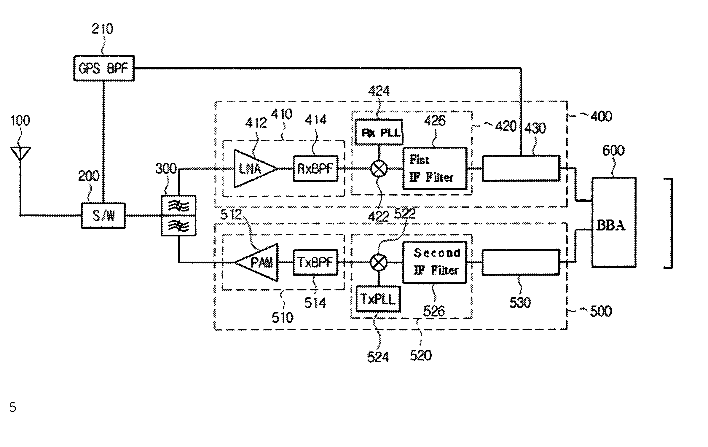
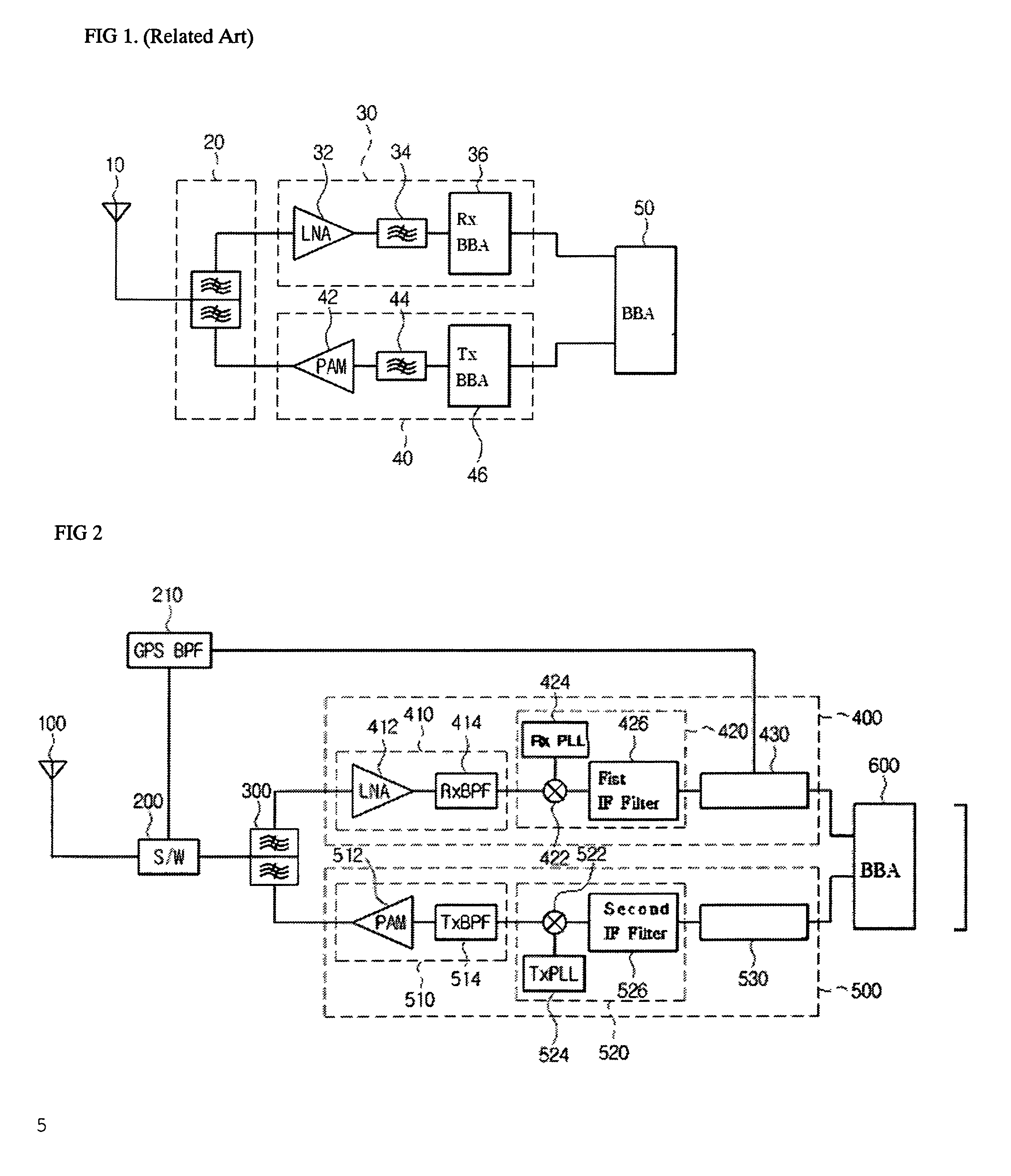
[0077]FIG. 2 is a circuit block diagram of an FEM according to a first embodiment of the present invention;

[0078]Referring to FIG. 2, an FEM according to a first embodiment of the present invention includes a duplexer 300, a receiver 400 and a transmitter 500. The receiver 400 includes a radio frequency (RF) receiving unit 410 having low noise amplifier (LNA) 412 and a receiving band pass filter (Rx BPF) 414, an intermediate frequency (IF) receiving unit 420 having a first mixer 422 and a first phase locked loop circuit 424 and an First IF Filter 426, and a receiving process unit 430.

[0079]The transmitter 500 includes an RF transmitting unit 510 having a PAM 512 and a transmitting band pass filter (Tx BPF) 514, an IF transmitting unit 520 having a second mixer 522 and a second phase locked loop circuit 524 and a second IF filter 526, and a transmitting process unit 530.

[0080]The duple...

second embodiment

[0112]FIG. 5 is a circuit block diagram of an FEM according to a Second embodiment of the present invention;

[0113]Referring to FIG. 5, an FEM according to a first embodiment of the present invention includes a duplexer 300, a receiver 400 and a transmitter 500. The FEM of the second embodiment is similar to that of the first embodiment.

[0114]Comparing a first embodiment of the present invention, the second embodiment of the present invention comprises further an inductor 110 that is connected to an antenna terminal of the duplexer 300 and a load switch 220 that is connected to the PAM 512,

[0115]Referring to FIG. 5, the load switch 220 functions to turn on and off the amplifier of the PAM 512.

[0116]The load switch 220 may be provided as a separated switch device or as a switching circuit having a resistor, a switching transistor, a capacitor, and a diode.

[0117]The load switch 220 receives a control signal of the base band process unit 600 and turns on and off a main power of the PAM ...

third embodiment

[0165]A FEM according to a third embodiment of the present invention will now be described. The FEM according to the third embodiment of the present invention is a communication module having a diversity receiving unit, which is mounted in a mobile communication device and process the communication using CDMA 1xEV-DO standard.

[0166]FIG. 17 is a schematic block diagram of an FEM according to a first embodiment of the present invention.

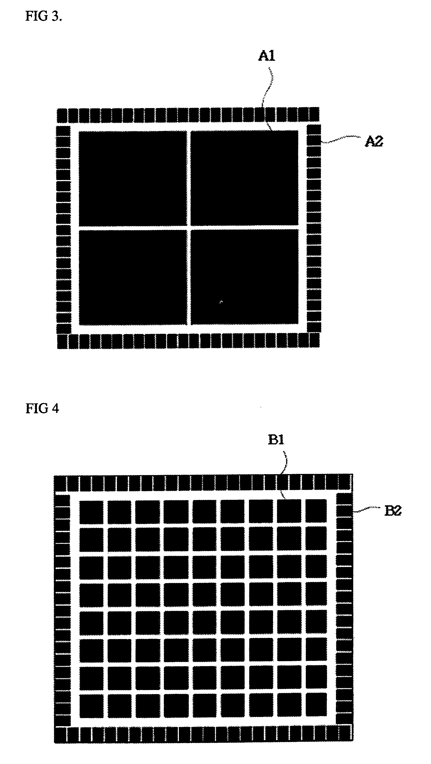
[0167]Referring to FIG. 17, a FEM 190 according to a third embodiment of the present invention includes a duplexer 105, a PAM 111, a transmitting filter 115, a transmitting process unit 130, a first receiving filter 120, a second receiving filter 121, a first receiving process unit 140, a second receiving process unit 150, and a GPS filter 125. These components are manufactured as separated components and mounted in the form of MCM.

[0168]The MCM mounting structure will be described later with reference to FIG. 18.

[0169]The duplexer 105 is a major passin...


PUM


Abstract

A front end module includes a multilayered structure. The multilayered structure includes a transmitter, a receiver, and a duplex unit. The multilayered structure further includes a ground layer. The ground layer includes a ground pattern having at least one block on a surface of a substrate of the front end module.

Description

BACKGROUND OF THE INVENTION[0001]1. Field of the Invention[0002]The present invention relates to a front end module used in a mobile communication device.[0003]2. Description of the Related Art[0004]The front end module (FEM) is a transmitting / receiving device used in a mobile communication device to control an electric wave signal. The FEM is a complex component on which a plurality of electronic components is mounted in a single substrate.[0005]For example, a conventional FEM for processing a code division multiple access (CDMA) will now be described.[0006]FIG. 1 is a circuit block diagram of a conventional CDMA FED.[0007]Referring to FIG. 1, a conventional CDMA FEM includes a duplexer 20, a receiver 30, and a transmitter 40. The transmitter 40 includes a transmitting process module 46 (a Tx BBA or RF transmitter), transmitting filter 44, and a power amplifier module (PAM) 42. The receiver 30 includes a low noise amplifier (LNA) 32, a receiving filter 34, and an receiving process ...

Claims


Application Information

Patent Timeline
Patent Type & Authority Patents(United States)
IPC IPC(8): H05K7/02H05K7/06H05K7/08H05K7/10
CPCH04B1/52H04L27/0002H01L2224/49171H01L2224/73265H01L2224/48091H01L2224/32145H01L2924/00014
Inventor KIM, KYUNG JOONNAM, HYOUNG KILEE, WON GYU
Owner LG INNOTEK CO LTD
Why Eureka
Try Eureka