Gallium nitride-based semiconductor stacked structure, production method thereof, and compound semiconductor and light-emitting device each using the stacked structure

a technology of gallium nitride and stacked structure, which is applied in the direction of semiconductor lasers, coatings, lasers, etc., to achieve the effect of convenient production, convenient production and convenient production

Active Publication Date: 2010-08-10
TOYODA GOSEI CO LTD
View PDF13 Cites 5 Cited by
  • Summary
  • Abstract
  • Description
  • Claims
  • Application Information

AI Technical Summary

Benefits of technology

[0012]According to the present invention, there is provided a low-temperature-deposited buffer layer formed on a sapphire substrate and including a single-crystal layer of a junction area being in contact with the substrate, wherein the single-crystal layer is composed of a hexagonal AlXGaYN (0.5<X≦1, X+Y=1) single crystal, containing Al in a predominant amount with respect to Ga, such that the [2.−1.−1.0.] direction of the AlXGaYN crystal coincides with the a-axis of the sapphire substrate, thereby attaining a well-unified orientation.
[0028]According to the eighth or ninth aspect of the invention, a compound semiconductor device or a light-emitting device is fabricated from a stacked structure including a GaN-based semiconductor single-crystal layer having a well-unified orientation. The invention is applicable to provision of semiconductor devices, such as a light-emitting diode exhibiting excellent emission characteristics; i.e., causing few local breakdowns in the reverse voltage direction.

Problems solved by technology

However, the low-temperature-deposited buffer layer formed on a sapphire substrate has a drawback in that the orientation of the single-crystal layer included in the buffer layer is not sufficiently identical on the surface of the sapphire substrate, thereby failing to attain consistent formation, on the substrate, of a GaN-based Group III nitride semiconductor layer having the identically same orientation and excellent single-crystal characteristics.

Method used


Image

  • Gallium nitride-based semiconductor stacked structure, production method thereof, and compound semiconductor and light-emitting device each using the stacked structure
  • Gallium nitride-based semiconductor stacked structure, production method thereof, and compound semiconductor and light-emitting device each using the stacked structure
  • Gallium nitride-based semiconductor stacked structure, production method thereof, and compound semiconductor and light-emitting device each using the stacked structure

Examples


example 1

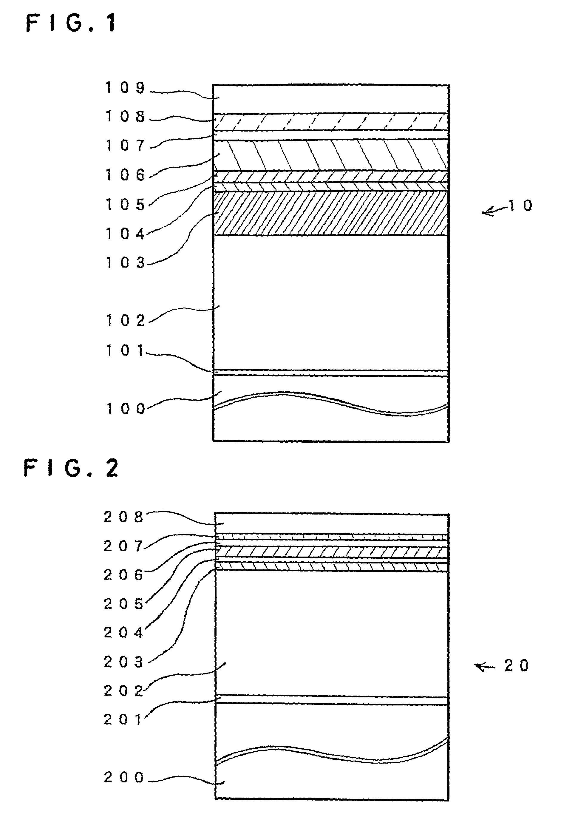
[0061]The present invention will next be described in detail by way of Example 1. In Example 1, a GaN-based Group III nitride semiconductor layer was grown on a sapphire substrate by the mediation of a low-temperature-deposited buffer layer including a single-crystal layer to thereby fabricate a GaN-based semiconductor stacked structure 10.

[0062]FIG. 1 is a schematic cross-sectional view of the GaN-based semiconductor stacked structure 10 of Example 1.

[0063]Group III nitride semiconductor layers 102 to 109 included in the GaN-based semiconductor stacked structure 10 were formed on a (0001) surface of a sapphire substrate 100 by the mediation of a low-temperature-deposited buffer layer 101 composed of an aluminum gallium nitride mixed crystal (Al0.90Ga0.10N).

[0064]The low-temperature-deposited buffer layer 101 was grown through an atmospheric pressure (near atmospheric pressure) MOCVD by use of trimethylaluminum ((CH3)3Al) as an aluminum (Al) source, trimethylgallium ((CH3)3Ga) as a ...

example 2

[0076]The present invention will next be described in detail by way of Example 2. In Example 2, a GaN-based Group III nitride semiconductor layer different from that of Example 1 was grown on a sapphire substrate by the mediation of a low-temperature-deposited buffer layer having a composition different from that employed in Example 1 to thereby fabricate a GaN-based semiconductor stacked structure 20.

[0077]FIG. 2 is a schematic cross-sectional view of the GaN-based semiconductor stacked structure 20 of Example 2.

[0078]Group III nitride semiconductor layers 202 to 208 included in the GaN-based semiconductor stacked structure 20 were formed on a (0001) surface of a sapphire substrate 200 by the mediation of a low-temperature-deposited buffer layer 201 composed of aluminum nitride (AlN). The low-temperature-deposited buffer layer 201 was grown through a reduced-pressure MOCVD by use of tri(isobutyl)aluminum ((i-C4H9)3Al) as an aluminum (Al) source and ammonia (NH3) as a nitrogen (N) s...

example 3

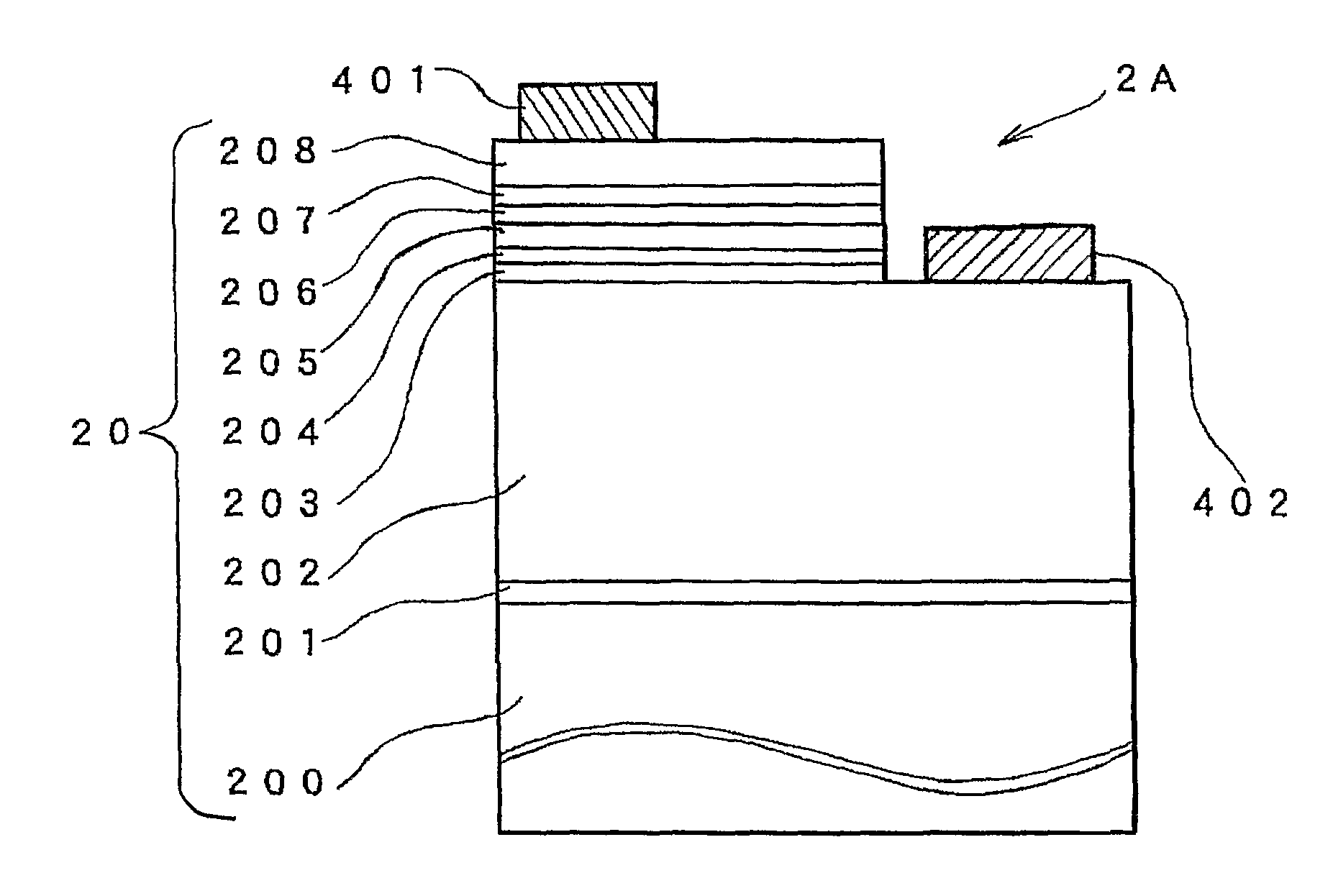
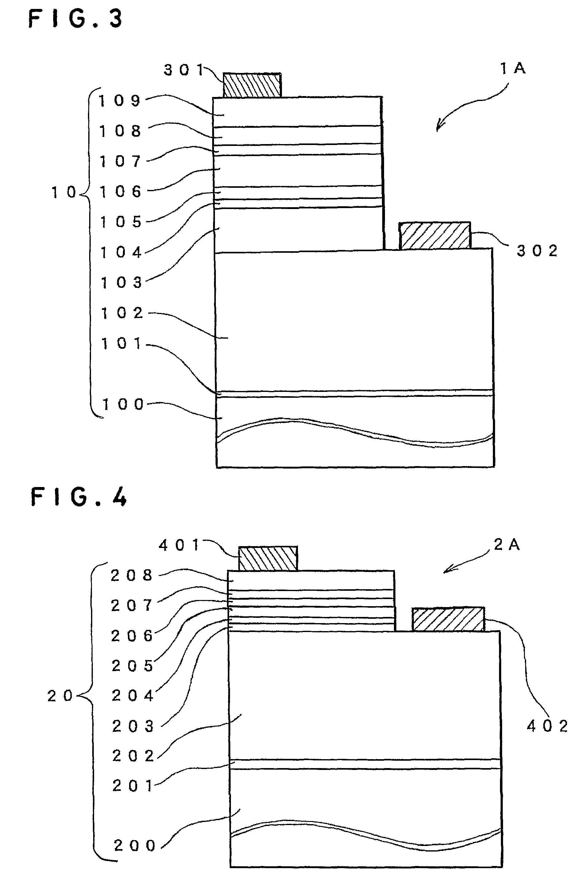
[0089]The present invention will next be described in detail by way of Example 3, in which an LED 1A was fabricated from the GaN-based semiconductor stacked structure 10 of Example 1.

[0090]FIG. 3 is a schematic cross-sectional view of the LED 1A of Example 3.

[0091]The GaN-based semiconductor stacked structure 10 of Example 1 was processed through a conventional plasma etching means, whereby a portion of the surface of the n-type GaN layer 102 provided by the mediation of the low-temperature-deposited buffer layer 101 was exposed, the portion being exclusively an area where an n-type Ohmic electrode 302 was to be provided. Subsequently, on the thus exposed surface of the n-type GaN layer 102, aluminum (Al)—vanadium (V) alloy film and Al film were sequentially stacked, thereby providing the n-type Ohmic electrode 302. On a corner portion of the p-type Al0.05Ga0.95N layer 109 serving as a surface of the stacked structure 10, gold (Au)—chromium (Cr)—cobalt (Co) alloy film and Au—Cr allo...


PUM

PropertyMeasurementUnit
thicknessaaaaaaaaaa
thicknessaaaaaaaaaa
lattice spacingaaaaaaaaaa

Abstract

A gallium-nitride-based semiconductor stacked structure includes a low-temperature-deposited buffer layer and an active layer. The low-temperature-deposited buffer layer is composed of a Group III nitride material that has been grown at low temperature and includes a single-crystal layer in an as-grown state, the single-crystal layer being present in the vicinity of a junction area that is in contact with a (0001) (c) plane of a sapphire substrate. The active layer is composed of a gallium-nitride (GaN)-based semiconductor layer that is provided on the low-temperature-deposited buffer layer. The single-crystal layer is composed of a hexagonal AlXGaYN (0.5<X≦1, X+Y=1) crystal that contains aluminum in a predominant amount with respect to gallium such that a [2.−1.−1.0.] direction of the AlXGaYN crystal orients along with a [2.−1.−1.0.] direction of the (0001) bottom plane of the sapphire substrate.

Description

CROSS REFERENCE TO RELATED APPLICATIONS[0001]This application is an application filed under 35 U.S.C.§111(a) claiming the benefit pursuant to 35 U.S.C.§119(e)(1) of the filing dates of Provisional Application No. 60 / 577,576 filed Jun. 8, 2004 and Japanese Patent Application No. 2004-157132 filed May 27, 2004 pursuant to 35 U.S.C.§111(b).TECHNICAL FIELD[0002]The present invention relates to a gallium-nitride-based semiconductor stacked structure having a specific low-temperature-deposited buffer layer (i.e., buffer layer formed at relatively low temperature) advantageous for enhancing orientation characteristics of a gallium-nitride-based Group III-V compound semiconductor layer, to a method for producing the stacked structure, and to a compound semiconductor device and a light-emitting device each using the stacked structure.BACKGROUND ART[0003]Conventionally, gallium nitride (GaN)-based Group III-V compound semiconductors of cubic zinc-blende crystal type or Wurtzite crystal type a...

Claims


Application Information

Patent Timeline
Patent Type & Authority Patents(United States)
IPC IPC(8): H01L31/153H01L29/165C23C16/34H01L33/16H01L21/20H01L21/205H01L33/06H01L33/12H01L33/20H01L33/32H01L33/40H01S5/323
CPCH01L21/0242H01L21/02433H01L21/02458H01L21/02516H01L21/0254H01L21/02609H01L21/0262H01L33/007H01L33/16H01L33/32
Inventor UDAGAWA, TAKASHI
Owner TOYODA GOSEI CO LTD
Why Eureka
Try Eureka