

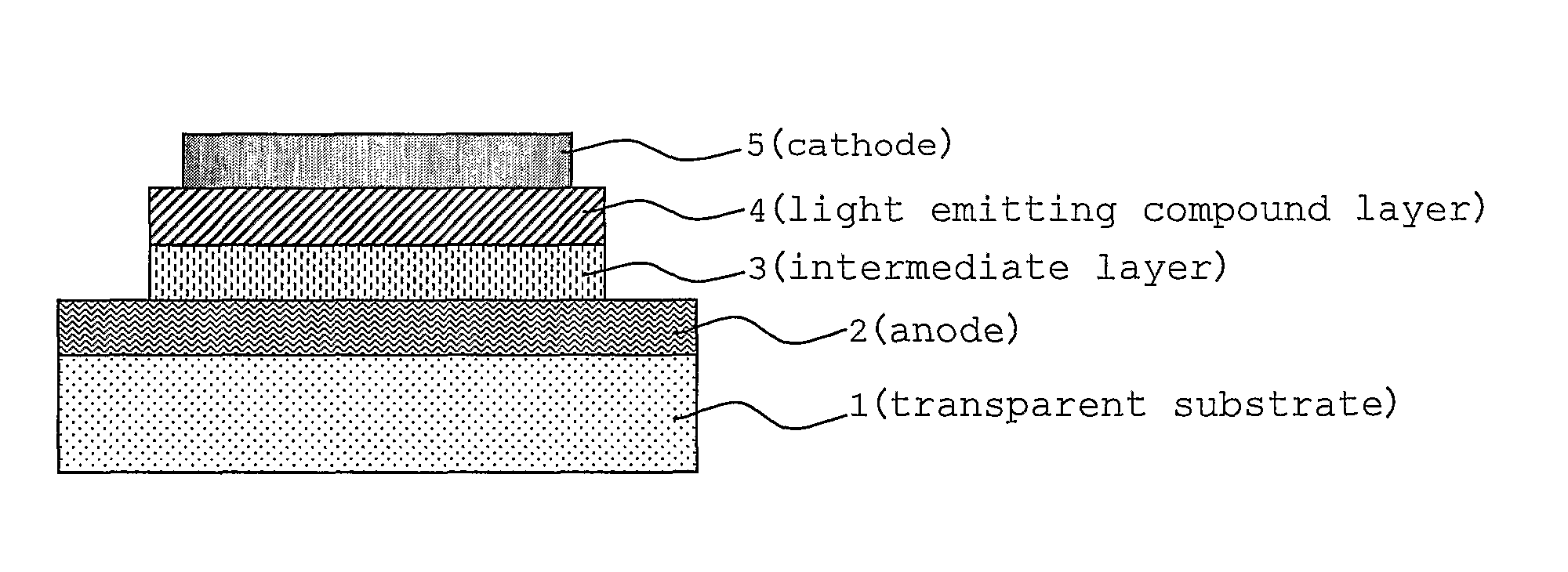
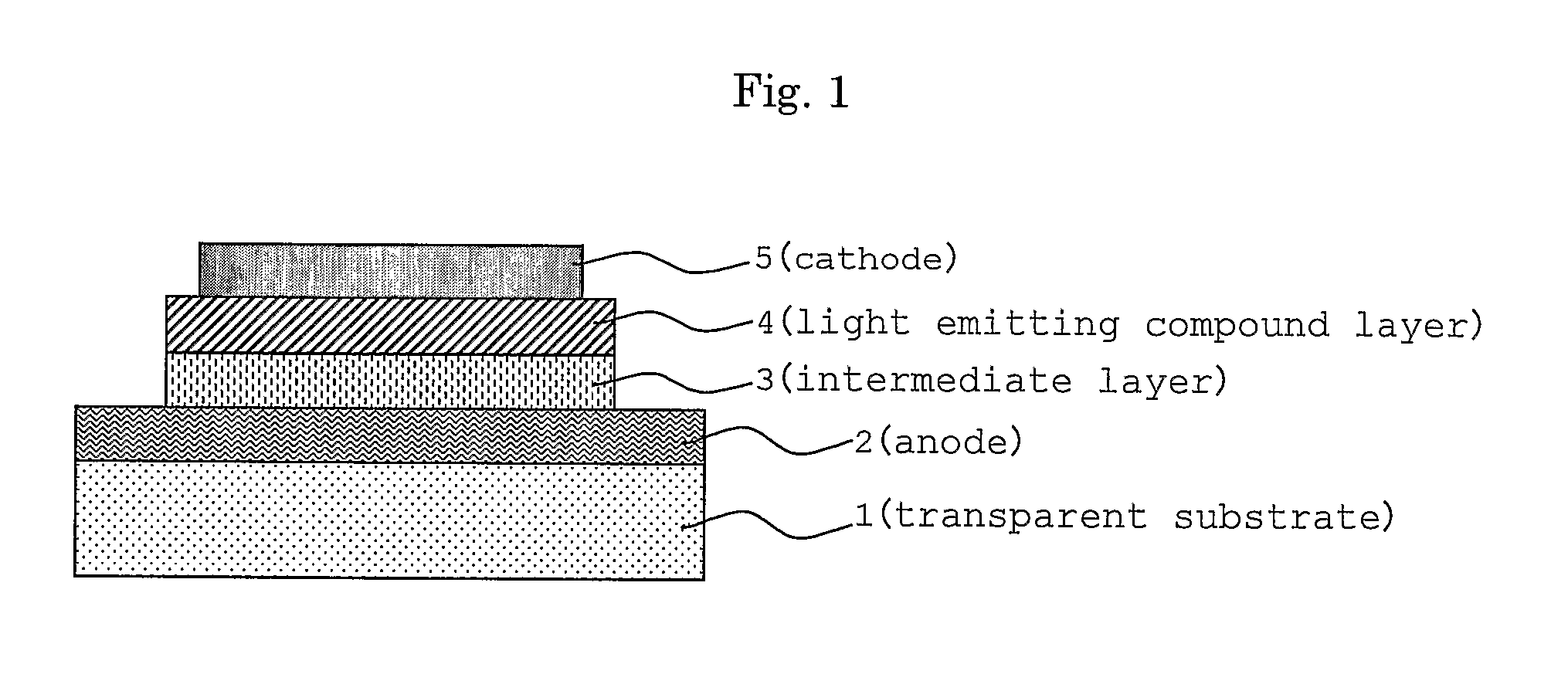
Organic electroluminescent device and production method thereof
a technology of electroluminescent devices and production methods, applied in the direction of organic semiconductor devices, discharge tube luminescnet screens, natural mineral layered products, etc., can solve the problems of increasing the driving voltage, insufficient current-voltage properties and a lower operating stability, and the need for vacuum apparatuses, etc., to achieve high maximum luminance and long life
- Summary
- Abstract
- Description
- Claims
- Application Information
AI Technical Summary
Benefits of technology
Problems solved by technology
Method used
Image

Examples
example 1
[0095]A substrate with ITO was subjected to liquid cleaning followed by a oxygen plasma cleaning processing in the same manner as in Reference Example to prepare a substrate coated with a conventional intermediate layer. The thickness of the obtained a conventional intermediate layer and the surface roughness of the obtained substrate coated with a conventional intermediate layer was measured and as a result of this, the film thickness was 50 nm, the Ra value was 0.7 nm and the height of projection was 9 nm. Next, the substrate coated with a conventional intermediate layer was optimized. That is, the substrate coated with a conventional intermediate layer was fixed on a spin coater and IPA was dropped thereon while spinning it at 3000 rpm to clean the substrate. The cleaning was carried out for 1 minutes. After dropping, the substrate was further spun at 4000 rpm for 1 minutes and then dried at 200° C. for 1 minutes. The obtained intermediate layer after optimization had a film thic...
example 2
[0096]A substrate with ITO dried after liquid cleaning in a same manner as in Comparative Example 1 was placed into a plasma generator, and oxygen gas was supplied into the apparatus. By applying an alternating voltage into the apparatus, discharge was initiated and then oxygen plasma was generated to expose the substrate with ITO. That is, the oxygen gas flow rate supplying into the apparatus was controlled to be a pressure of 1 Pa. The plasma processing was carried out at 150 W of supplied electric power for 30 seconds. Next, the supplying gas was changed from oxygen gas to CHF3 gas and the flow rate was controlled to be a pressure of 7 Pa. Then, the plasma processing of the substrate was carried out at 300 W of supplied electric power for 10 seconds in PE mode. As a result of an X-ray photoelectron spectroscopy (XPS) analysis of the surface of the substrate with ITO after the process, it was found that a fluorocarbon film (described as “CFn intermediate layer” in Table 1) was for...
example 3
[0098]A substrate with ITO dried after liquid cleaning in a same manner as in Comparative Example 1 was placed into a plasma generator, and oxygen gas was supplied into the apparatus. By applying an alternating voltage into the apparatus, discharge was initiated and then oxygen plasma was generated to expose the substrate with ITO. The oxygen gas flow rate supplying into the apparatus was controlled to be a pressure of 1 Pa. The plasma processing was carried out 150 W of supplied electric power for 30 seconds. Next, the supplying gas was changed from oxygen to CHF3 gas and the flow rate was controlled to be a pressure of 7 Pa. Then, the plasma processing of the substrate was carried out at 100 W of applied electric power for 10 seconds in PE mode. As a result of an X-ray photoelectron spectroscopy (XPS) analysis of the surface of the substrate with ITO after the process, it was found that a fluorocarbon film was formed on the surface of the substrate with ITO. It was further found t...
PUM
| Property | Measurement | Unit |
|---|---|---|
| thickness | aaaaa | aaaaa |
| Ra | aaaaa | aaaaa |
| height | aaaaa | aaaaa |
Abstract
Description
Claims
Application Information