Chemical sensors using coated or doped carbon nanotube networks

a carbon nanotube and network technology, applied in the field of chemical sensors, can solve the problems of difficult to make a single swcnt grow horizontally in order to bridge a given distance between the source and the drain, and the platform faces serious commercialization difficulties,

Active Publication Date: 2010-09-21
NASA
View PDF8 Cites 19 Cited by
  • Summary
  • Abstract
  • Description
  • Claims
  • Application Information

AI Technical Summary

Benefits of technology

[0008]These needs are met by the invention, which provides a chemical sensor or sensor array for detecting presence, at or near room temperature, of one or more of N target gas components or molecules (N≧1) in a gas mixture contained in a chamber, by any ambient being considered. The sensor contains a network of SW

Problems solved by technology

This platform faces some serious difficulties for commercialization.
First, the CNT-FET requires semiconducting SWCNTs for its operation, and selective growth of metallic versus semiconducting nanotubes is not possible today.
Second, if an in situ chemical vapor deposition (“CVD”) process is used in the device f

Method used


Image

  • Chemical sensors using coated or doped carbon nanotube networks
  • Chemical sensors using coated or doped carbon nanotube networks
  • Chemical sensors using coated or doped carbon nanotube networks

Examples


Embodiment Construction

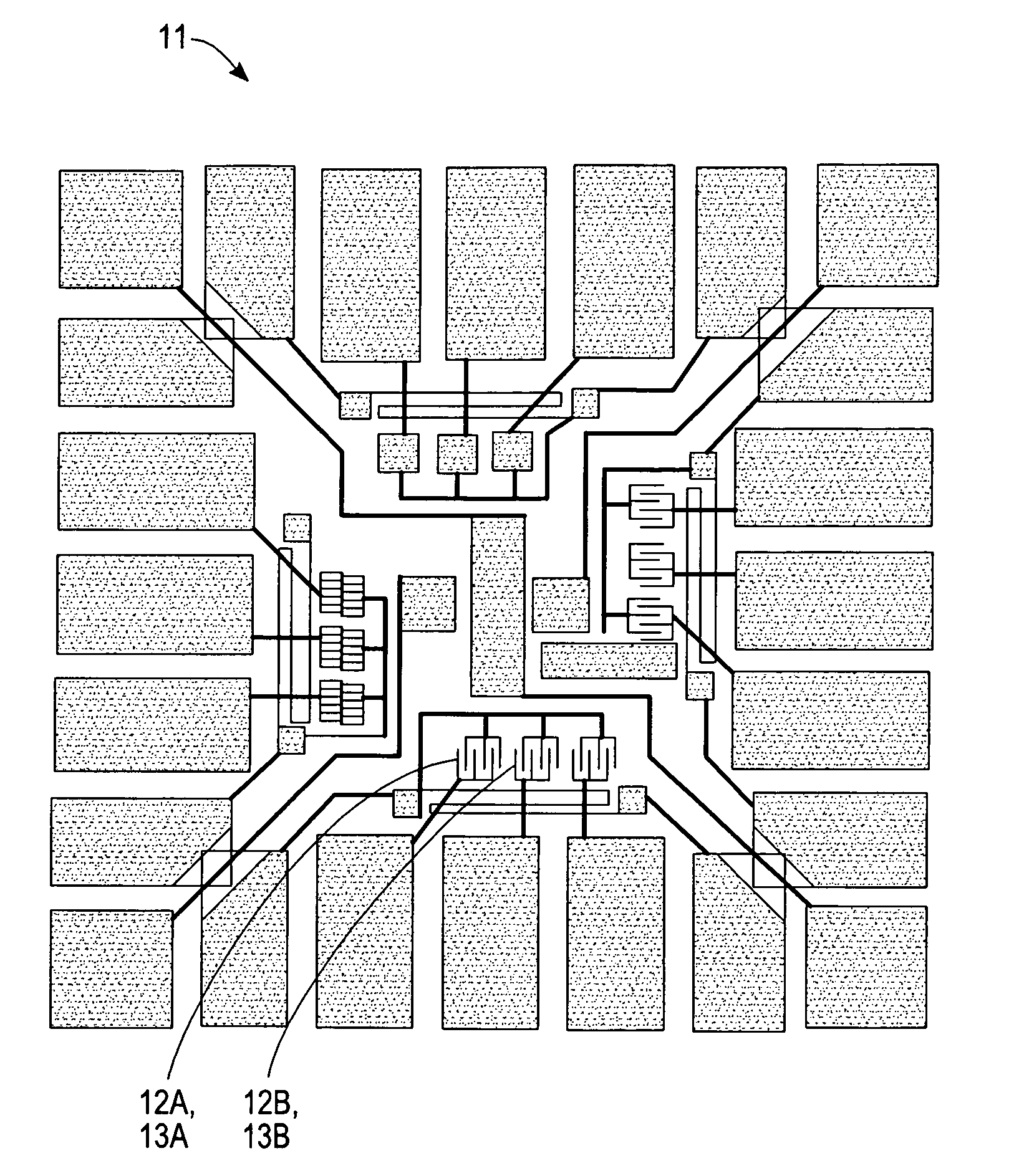
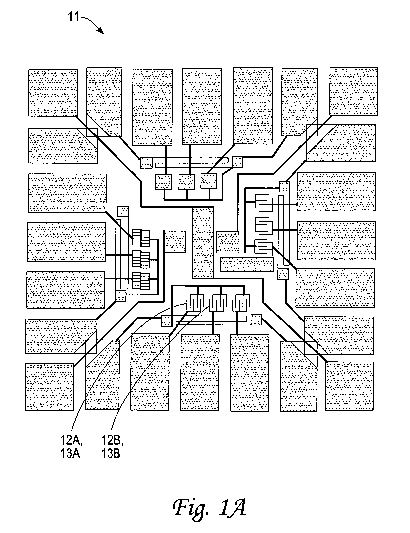
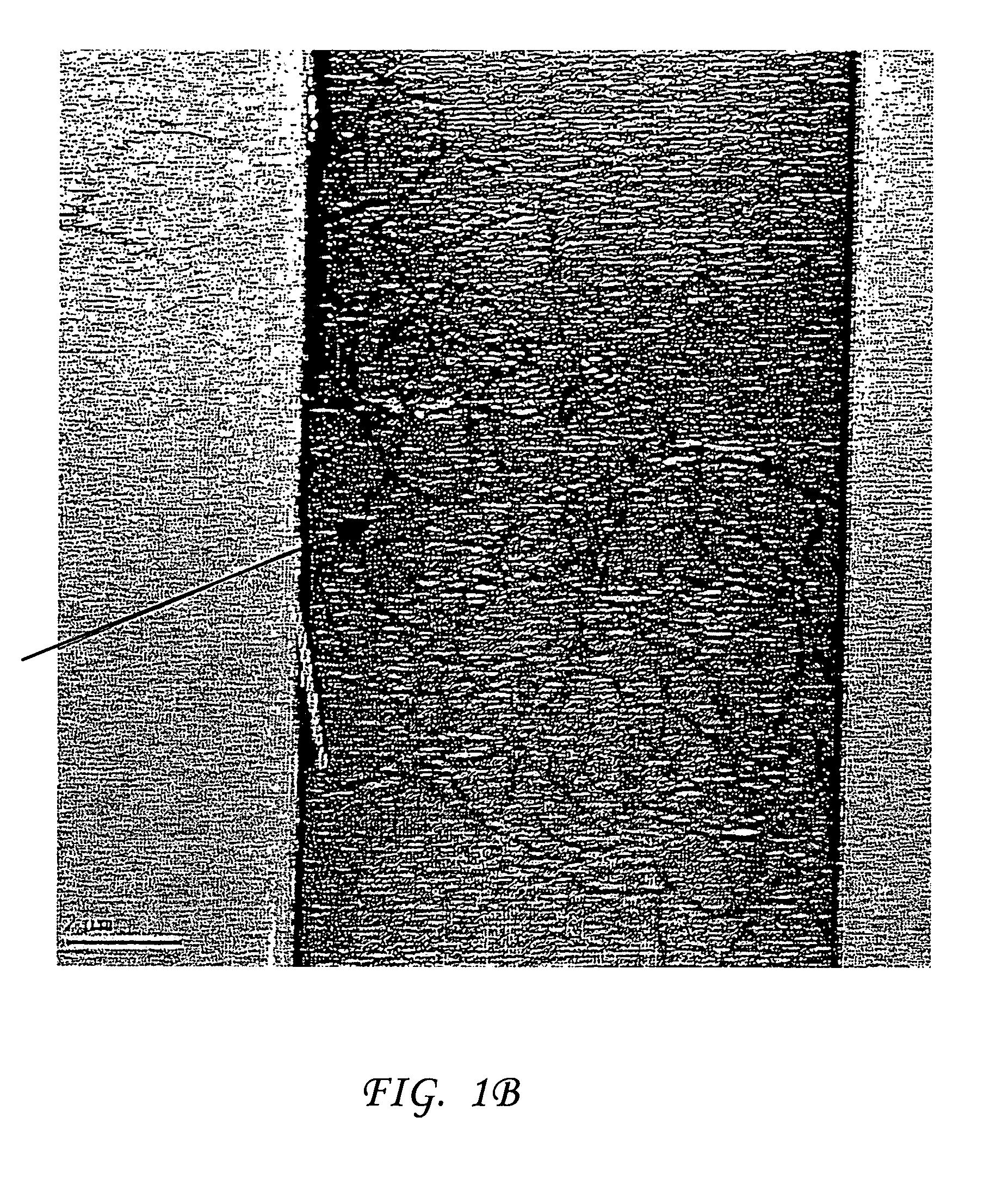
[0020]FIGS. 1A and 1B illustrate a sensor 11, constructed according to the invention, including interdigitated electrode fingers (“IDEFs”), 12A and 12B, with corresponding fingers, connected to respective first and second voltage sources, 13A and 13B, with a controllable voltage difference. In FIG. 1A, a 1 cm×1 cm chip with Q sensing elements and SWCNTs bridging the gaps between adjacent IDEFs (herem Q=2-12). Each IDE was fabricated using conventional photolithography with a nominal finger width of 10 μm and gap sizes of 4, 8, 12 and 50 μm, or any other desired set of gap sizes. The fingers and contact pads, 11A-i and 11B-j, were thermally evaporated Ti (20 nm thickness) and Pt (200 nm thickness) on a layer of SiO2, thermally grown on a silicon substrate. The sensing material was bulk-produced SWCNTs from a HiPCo process (Rice University.), purified to remove amorphous carbon and metal impurities according to a procedure described in the literature. The purified SWCNTs were disperse...


PUM


Abstract

Methods for using modified single wall carbon nanotubes (“SWCNTs”) to detect presence and/or concentration of a gas component, such as a halogen (e.g., Cl2), hydrogen halides (e.g., HCl), a hydrocarbon (e.g., CnH2n+2), an alcohol, an aldehyde or a ketone, to which an unmodified SWCNT is substantially non-reactive. In a first embodiment, a connected network of SWCNTs is coated with a selected polymer, such as chlorosulfonated polyethylene, hydroxypropyl cellulose, polystyrene and/or polyvinylalcohol, and change in an electrical parameter or response value (e.g., conductance, current, voltage difference or resistance) of the coated versus uncoated SWCNT networks is analyzed. In a second embodiment, the network is doped with a transition element, such as Pd, Pt, Rh, Ir, Ru, Os and/or Au, and change in an electrical parameter value is again analyzed. The parameter change value depends monotonically, not necessarily linearly, upon concentration of the gas component. Two general algorithms are presented for estimating concentration value(s), or upper or lower concentration bounds on such values, from measured differences of response values.

Description

ORIGIN OF THE INVENTION[0001]This invention was made, in part, by one or more employees of the U.S. government. The U.S. government has the right to make, use and / or sell the invention described herein without payment of compensation therefor, including but not limited to payment of royalties.FIELD OF THE INVENTION[0002]This invention relates to use of carbon nanotube networks as sensors of chemical substances.BACKGROUND OF THE INVENTION[0003]Chemical sensors have been developed for decades now to detect gases and vapors at various concentration levels for deployment in a wide range of industrial applications. The detection usually centers on a change of a particular property or status of the sensing material (such as temperature, electrical, optical characteristics, etc.) upon exposure to the chemical species of interest. The selection of sensing material itself has spanned across the periodic table with a range of inorganic, semiconducting elements and organic compounds either in ...

Claims


Application Information

Patent Timeline
IPC IPC(8): G01N31/00
CPCG01N27/127Y10S977/92Y10S977/921Y10S977/922Y10S977/938
Inventor LI, JINGMEYYAPPAN, MEYYA
Owner NASA
Why Eureka
Try Eureka