Perfluoropolyether copolymer composition for forming banks

a technology of perfluoropolyether and composition, applied in the direction of thermoelectric device junction materials, electrical apparatus, solid-state devices, etc., can solve the problems of deterioration of the performance of the organic thin film transistor, degradation of the characteristics of the device, and degradation of the characteristics of the adjacent organic electronic device, so as to prevent or reduce the degradation of the organic film and increase the definition of the ink material

Active Publication Date: 2010-10-26
SAMSUNG ELECTRONICS CO LTD
View PDF11 Cites 5 Cited by
  • Summary
  • Abstract
  • Description
  • Claims
  • Application Information

AI Technical Summary

Benefits of technology

[0010]Therefore, example embodiments have been made in view of the problems of the prior art, and example embodiments provide a copolymer that may prevent or reduce degradation of an organic film and may ensure increased definition of an ink material to be filled between banks.
[0011]Example embodiments provide a composition for forming banks which may include the copolymer. Example embodiments provide a method for forming banks in the fabrication of an organic electronic device by a printing technique wherein pixel regions of adjacent organic electronic devices may not be adversely affected by an ink material, thus preventing or reducing deterioration of the characteristics of the adjacent organic electronic devices. Example embodiments also provide an organic thin film transistor which may include banks formed using the composition. Example embodiments provide a variety of electronic devices comprising the organic thin film transistor.

Problems solved by technology

However, when a liquid material (an ink material) is filled and a thin film pattern is formed to fabricate an organic electronic device by a solution processing technique, there may arise problems that the liquid material overflows and is introduced into pixel regions of adjacent organic electronic devices, resulting in degradation of the characteristics of the adjacent organic electronic devices.
For example, when a photoresist using an organic solvent is used to form banks in the fabrication of a bottom contact type or top gate type organic thin film transistor, overflow of the organic solvent may lead to degradation of an organic insulating film, resulting in deterioration of the performance of the organic thin film transistor.
However, the disadvantage of these methods may be that when organic electronic devices are fabricated using bottom gate type insulating films, which may be general structures of display arrays, they may be exposed to organic solvents, e.g., solvents of bank materials, photoresist solvents, developing solvents and / or photoresist strippers, causing degradation in the characteristics of the devices.
Because organic solvents of ink materials used to fabricate organic electronic devices have a decreased surface contact angle, the ink materials to be filled between banks may exhibit decreased definition for the banks, resulting in deteriorated performance of the devices.

Method used


Image

  • Perfluoropolyether copolymer composition for forming banks
  • Perfluoropolyether copolymer composition for forming banks
  • Perfluoropolyether copolymer composition for forming banks

Examples


synthesis example 1

Synthesis of Copolymers

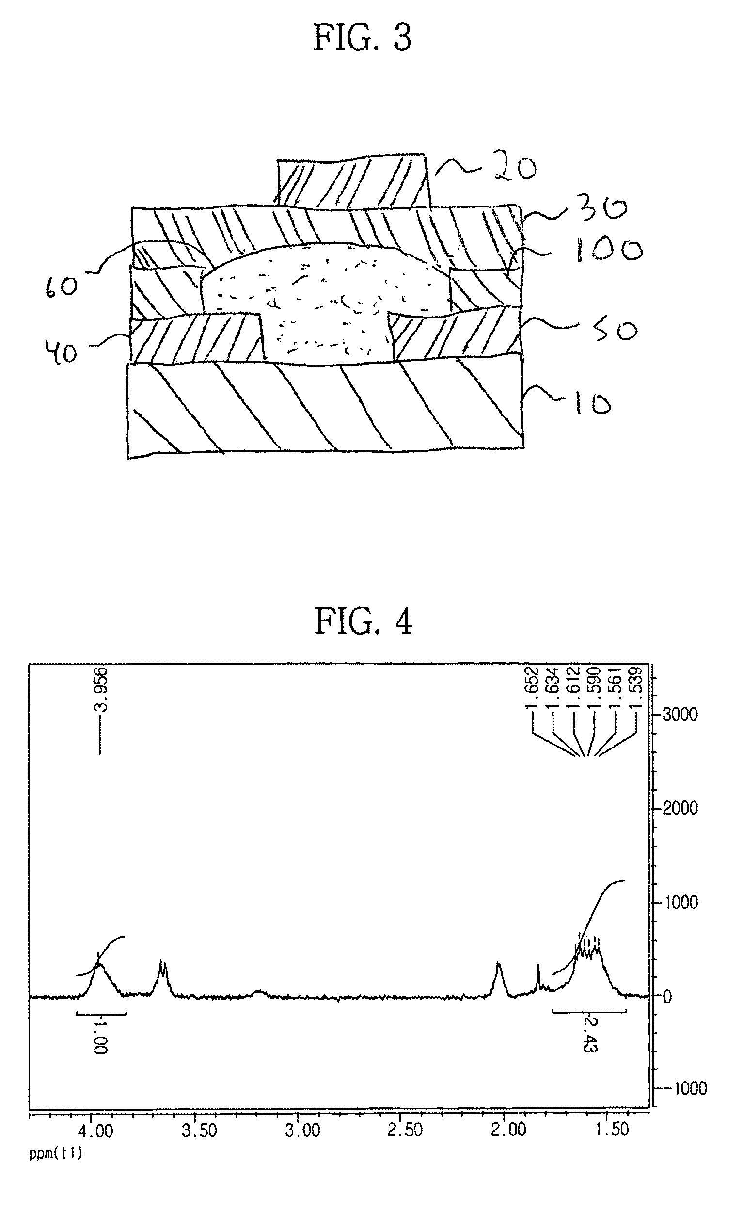
[0095]As depicted in Reaction 1, PFPE-Si(OEt)3 of Formula 3 was mixed with polyvinyl alcohol (#2000, Kanto Chemical Co.) as a photosensitive polymer in accordance with the compositions shown in Table 1. The mixtures were stirred and extracted with a fluorinated organic solvent (Vertrel XF®, DuPont). The obtained extracts were washed to give copolymers. The structure of the copolymers was identified by 1H-NMR spectroscopy. FIG. 4 shows the 1H-NMR spectrum of the copolymer in which the ratio of molar equivalents of the PFPE-Si(OEt)3 to the molar equivalents of the photosensitive polymer was about 0.05:1. The ratio of the number of hydrogen atoms contained in the hydroxyl groups to the number of secondary hydrogen atoms contained in the aliphatic chain was about 1:2.04 in pure polyvinyl alcohol, while the ratio was about 1:2.43 in the copolymer, which is apparent from the spectrum of FIG. 4. These results indicate that some hydroxyl groups of the polyvinyl alcoho...

example 1

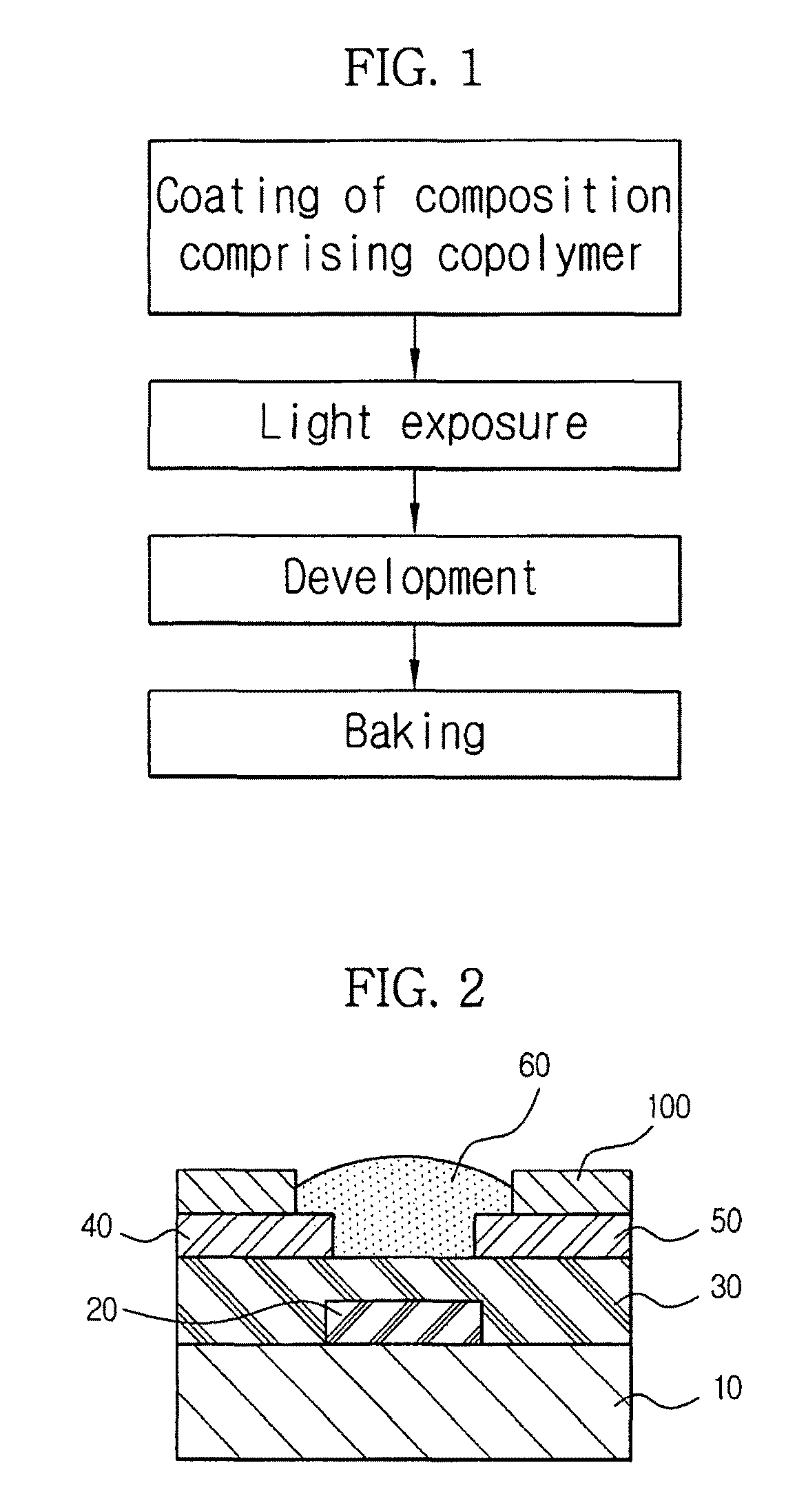
[0097]A glass substrate was cleaned, and aluminum (Al) was deposited thereon by a sputtering technique to form a gate electrode having a thickness of about 1,500 Å. An organic gate insulating film was formed to a thickness of about 4,000 Å on the gate electrode and the glass substrate by spin coating at about 2,000 rpm, followed by sequential baking at about 70° C. for about 20 minutes and about 200° C. for about 2 hours. Au was deposited on the gate insulating film to a thickness of about 700 Å by a thermal evaporation method, and was then subjected to a photolithographic process to form an Au electrode pattern. The deposition was conducted under a vacuum pressure of about 2×10⁻⁷ torr and a deposition rate of about 5 Å / sec.

[0098]Subsequently, banks were formed on the Au electrodes in accordance with the following procedure. Ammonium dichromate (Sigma Aldrich) was added to an about 5 wt % solution of each of the PFPE-polyvinyl alcohol copolymers in deionized water to prepare a coati...

experimental example 1

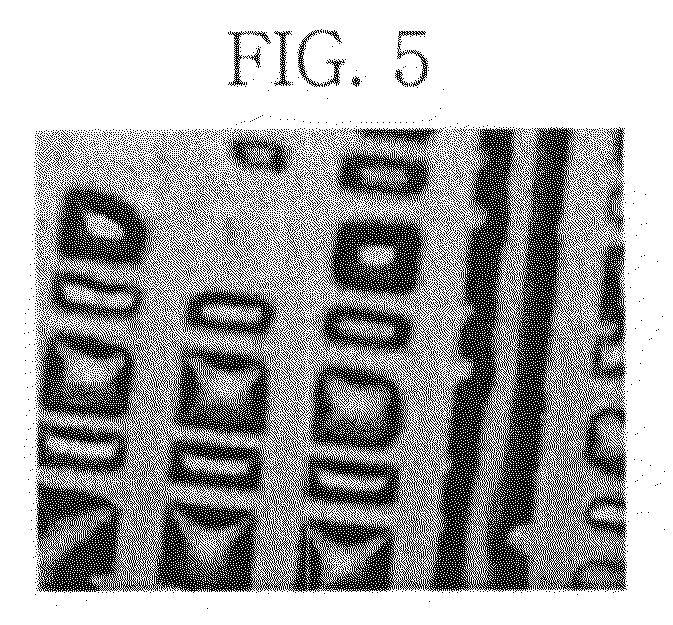
[0102]To evaluate the patternability of banks formed by the method of example embodiments, the size of the banks formed in Example 1 was measured using a confocal laser scanning microscope (OLYMPUS LEXT OLS3000). The results are shown in FIG. 5.

[0103]As apparent from the foregoing, the composition for forming banks according to example embodiments may include a copolymer of a perfluoropolyether derivative as a fluorinated surface modifier and a photosensitive polymer. Because the copolymer serves to minimize or reduce the surface energy of the composition, an ink material to be filled between banks may exhibit increased definition for the banks despite a decreased surface contact angle of an organic solvent of the ink material.

[0104]The use of a water-soluble photosensitive polymer, not having an influence on an organic insulating film, may enable the prevention or reduction of deterioration in the performance of an organic thin film transistor.

[0105]Where a simple mixture of a wate...


PUM

PropertyMeasurementUnit
wavelengthaaaaaaaaaa
poweraaaaaaaaaa
pressureaaaaaaaaaa

Abstract

Disclosed are a copolymer of a perfluoropolyether derivative and a photosensitive polymer, a composition for forming banks comprising the copolymer, and a method for forming banks using the composition. Also disclosed is an organic thin film transistor including the composition and an electronic device including the organic thin film transistor. The use of the copolymer may enable the formation of banks by a solution coating process. Because an organic thin film transistor including banks formed by the method may be fabricated without any degradation in the characteristics of the organic thin film transistor, improved electronic properties may be exhibited.

Description

PRIORITY STATEMENT[0001]This non-provisional application claims priority under 35 U.S.C. §119 to Korean Patent Application No. 10-2006-0095626, filed on Sep. 29, 2006, in the Korean Intellectual Property Office (KIPO), the entire contents of which are herein incorporated by referenceBACKGROUND[0002]1. Field[0003]Example embodiments relate to a copolymer, a composition for forming banks, and a method for forming banks using the composition. Other example embodiments relate to a copolymer of a perfluoropolyether derivative and a photosensitive polymer, a composition for forming banks comprising the copolymer, and a method for forming banks using the composition.[0004]2. Description of Related Art[0005]In recent years, polymeric materials have attracted increased attention as electrical and electronic materials in a wide variety of applications, e.g., functional electronic devices and optical devices, because of their ease of molding into fibers and films, improved flexibility, increas...

Claims


Application Information

Patent Timeline
Patent Type & Authority Patents(United States)
IPC IPC(8): C08L71/02G03F7/004
CPCC08G65/007C08L71/02G03F7/0046G03F7/032G03F7/033G03F7/04C08L29/04C08L2205/05G03F7/0757C08L2666/04C08K5/02C08K5/06
Inventor HAHN, JUNG SEOKIN, KYU YEOLKOO, BON WONHAN, KOOK MINLEE, SANG-YOON
Owner SAMSUNG ELECTRONICS CO LTD
Why Eureka
Try Eureka