
Method for fabricating an electronic device

a technology of electronic devices and manufacturing methods, applied in the direction of dielectric characteristics, light absorption dielectrics, conductive material removal by irradiation, etc., can solve the problems of rfid technology's use in inventory control, security, etc., and has serious financial ramifications, and can not meet the requirements of mass production of tags with required functionalities in a simple, reliable and consistent manner

Inactive Publication Date: 2010-11-23
IDEON LLC
View PDF5 Cites 17 Cited by
  • Summary
  • Abstract
  • Description
  • Claims
  • Application Information

AI Technical Summary

Benefits of technology

"The invention provides a process for making an electronic device by adding a layer of metal to a non-conductive surface and then using laser technology to create patterns of conductive and non-conductive areas. This process can be used to connect an electronic circuit to the metal layer. The invention also offers an alternative to the \"printed electronics\" approach for creating electronic circuitry or devices."

Problems solved by technology

Its use in inventory control, security, etc. for packaged goods has serious financial ramifications.
However, there are several roadblocks to the commercial use of RFID technology.
A key factor is the inability to mass produce tags with required functionalities in a simple, reliable, and consistent manner, and producing them cost effectively, for making widespread applications feasible.
Unfortunately, the currently available methods of tag manufacturing are not capable of meeting these requirements and therefore, the industry and the market, are at a stand still.
The cost of the antennae has been identified to be one of the key limiting variables and therefore, an intense effort is being made to overcome this problem.
The process is old, well understood and broadly practiced, however, wasteful, environmentally harmful, expensive, and therefore it is not able to take the industry to the next level.
However, none has been successful as a solution.
However, most of the solid state electronic circuitry is rigid and therefore, not suitable for use on packaging items, as most such items are flexible materials.
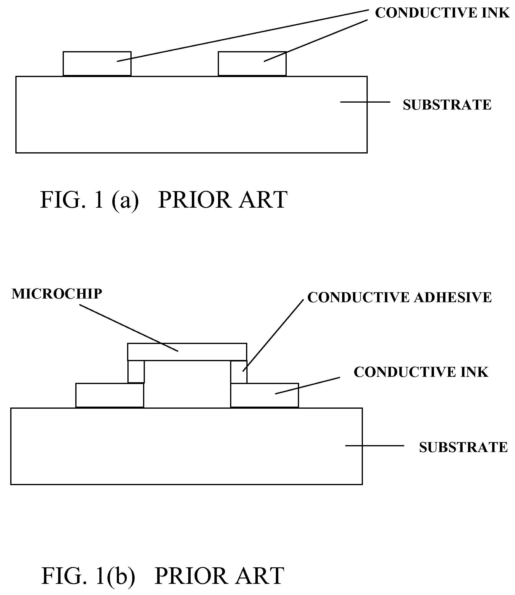
Therefore, a tremendous amount of effort is being used developing so called “printed electronics.” The goal of printed electronics is to print the required elements of an electrical circuitry onto the flexible substrate itself.
However, this process poses serious environmental and health and safety hazards.
This limits the number of substrates that can be used to print on, since only expensive substrates with high softening temperature may be used to avoid any deformation.
High temperature requirement also seriously reduces the overall productivity of the process.
Moreover, due to high loading of silver powder requirement, the ink formulations must contain extraneous additives, including volatile organic compounds (VOC), to produce inks in a printable fashion.
Although this process avoids any high temperature processing, it is a slow and wet process, with their inherent disadvantages.
While this approach promises to yield silver free, less expensive antennae, the productivity of such process is very low since UV laser irradiation has a limited energy level for ablating thicker metal layers and electrodeposition process is extremely slow and requires utilization of wet chemistry.
Lack of connection would further reduce the yield of the process and above all, reliability of the transponders itself.
Overall, the limitations of all the current and available approaches make the RFID antennae and transponders produced expensive, and limit their viability as commercially successful processes to satisfy projected industry needs for billions of inexpensive RFID transponders, for all types of applications including tagging of individual items.
Similarly, commercial manufacturing of microwave susceptors or sensors also face similar limitations.
However, this approach is complex.
In order to achieve a high enough conductivity at printed film thickness, mainly silver is used as metal, which is expensive.
The metal must also be in powder form with particle size ranging from micrometer to nanometer with their associated processing cost, further increasing the material cost.
The substrate must be able to withstand high bake temperature ˜130° C. without thermal distortion, and therefore can primarily be expensive polyesters with high glass transition temperature (Tg).
High web surface temperature requirement also slows down the overall printing process, increasing cost.
Therefore, materials are selected which would volatilize during the baking step, which in turn create undesired environmental (VOC) and health & safety issues.
In addition, despite the high heating step, the metal particles in the printed antenna simply do not attain their original metallic crystal structure and therefore results in printed antennae with somewhat reduced metal conductivity compared to their original value.
Any misalignment would increase waste factor and above all would increase unreliability of the system, increasing potential risks and security breaches in several sensitive application areas.
However, even with this approach there is at least 1-3% unreliability factor, which for mass adoption poses a great disadvantage.
The overall complexity, unreliability and economics of the current “printed antenna” process simply does not lend itself to be a solution to preventing the RFID market from achieving intended commercial success and there is a serious need for a new fabrication method for RFID antenna.

Method used


Image

  • Method for fabricating an electronic device
  • Method for fabricating an electronic device
  • Method for fabricating an electronic device

Examples


example 1

[0039]A 0.2 micron layer of aluminum was applied over a 50 micron thick polyethylene terephthalate (PET) film in a vacuum metallizer. The metallized PET was ablated with an IR laser from the metal side to form an image having a circular pattern. The electrical resistivity of this pattern was less then 1 ohm, which is sufficient for a typical radio-frequency antenna.

example 2

[0040]Example 1 was repeated except the metal layer was ablated by the IR laser from the opposite side, through the PET film, leading to same result as in Example 1.

example 3

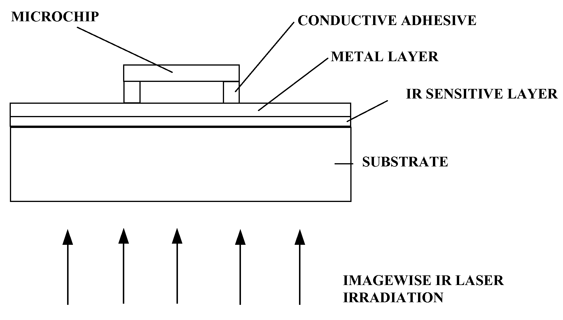
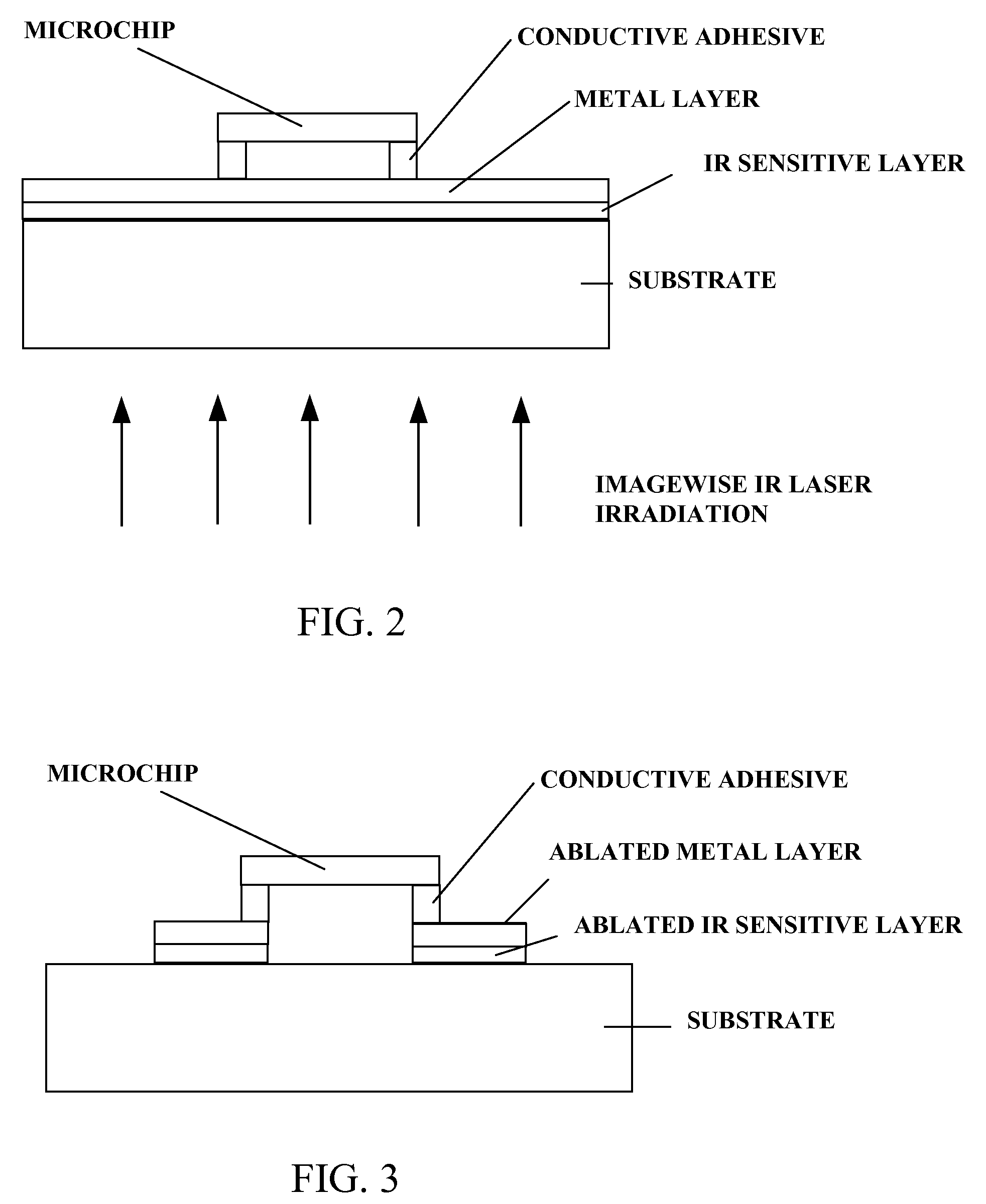
[0041]A number of computer chips suitable for 13.56 MHz RFID tags were attached with an adhesive to a metallized aluminum polypropylene film, with a metal optical density less than 2.0. The structure was exposed with an IR fiber laser from Lasercut Inc. (Branford, Conn.) from the back side of the metallized film surface, i.e., the side opposite to the side containing the computer chips. The laser exposure ablated the aluminum metal precisely and cleanly to form antenna geometry for 13.56 MHz transponder. The metal could be cleanly ablated right underneath the connecting pads for the chip, such that a fully functional and flexible antenna could be formed in one single step.


PUM

PropertyMeasurementUnit
thicknessaaaaaaaaaa
temperatureaaaaaaaaaa

Abstract

The invention provides an article and process for producing electronic devices. More particularly the invention relates to an article and process for fabricating patterns of electrically conductive materials on non-electrically conductive substrates by laser ablation. Such an article and process find use in the production of RDIF devices, antennae, electrical circuits, microwave susceptors, contacts, leads, conductors, interactive displays, electrostatic shielding devices and the like. The process involves first providing an electrically conductive metal layer on an electrically non-conductive substrate. Then an electronic circuit is electrically connected to the electrically conductive metal layer. Thereafter a portion of the electrically conductive metal layer is ablated with infrared laser radiation to form a pattern of electrically conductive areas and electrically non-conductive areas on the substrate, wherein at least a portion of the electrically conductive areas are electrically connected to the electronic circuit.

Description

CROSS REFERENCE TO RELATED APPLICATION[0001]This application claims the benefit of U.S. Provisional patent application Ser. No. 60 / 806,722, filed Jul. 6, 2006, which is incorporated herein by reference.BACKGROUND OF THE INVENTION[0002]1. Field of the Invention[0003]The present invention relates to an article and process for producing electronic devices. More particularly the invention relates to an article and process for fabricating patterns of electrically conductive materials on non-electrically conductive substrates by laser ablation. Such an article and process find use in the production of RFID devices, antennae, electrical circuits, microwave susceptors, contacts, leads, conductors, sensors, interactive displays, electrostatic shielding devices, heating elements and the like.[0004]2. Description of the Related Art[0005]There is great commercial interest in a new generation of data transmitting electronic devices such as transponders, sensors, etc. The use of electronic compon...

Claims


Application Information

Patent Timeline
Patent Type & Authority Patents(United States)
IPC IPC(8): H05K3/02
CPCH05K3/027H05K2201/0112H05K2203/1581Y10T29/49018Y10T29/4913Y10T29/49156Y10T29/49169
Inventor LAKSIN, MIKHAILCHATTERJEE, SUBHANKAR
Owner IDEON LLC
Learn More