Non-volatile memory device and method for fabricating the same

a memory device and non-volatile technology, applied in semiconductor devices, semiconductor/solid-state device details, electrical devices, etc., can solve the problems of deteriorating film quality, reducing charge retention time, and difficulty in adjusting the threshold voltage (vsub>t/sub>) to a desired level, so as to prolong the data retention time, improve reliability, and improve processing speed

Inactive Publication Date: 2010-12-14
SK HYNIX INC
View PDF89 Cites 14 Cited by
  • Summary
  • Abstract
  • Description
  • Claims
  • Application Information

AI Technical Summary

Benefits of technology

[0040]In one aspect, the present invention is directed to a non-volatile memory semiconductor device capable of exhibiting prolonged data retention time, high processing speed and improved reliability.

Problems solved by technology

However, the large thickness of the film makes it difficult to adjust a threshold voltage (Vt) to a desired level and requires a high voltage and power for programming.
When deterioration of the film quality of the silicon nitride film occurs due to a variation (e.g., thinness) in the thickness thereof, charge leakage increases thereby decreasing charge retention time.
As a result, the reliability of the memory device deteriorates.
When hafnia is deposited on alumina, sequential deposition of different kinds of oxide films involves a complicated fabrication process.
In addition, an equipment structure to realize such a process is complicated, and maintenance and management for mass-production become difficult.
Furthermore, these attempts involve a process for depositing an oxide film on the surface of a silicon substrate, thereby causing undesired oxidation on the surface of the silicon substrate.

Method used


Image

  • Non-volatile memory device and method for fabricating the same
  • Non-volatile memory device and method for fabricating the same
  • Non-volatile memory device and method for fabricating the same

Examples


Embodiment Construction

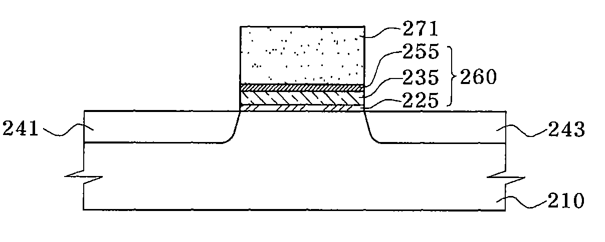
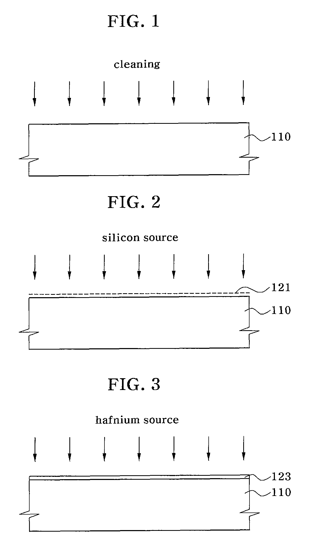
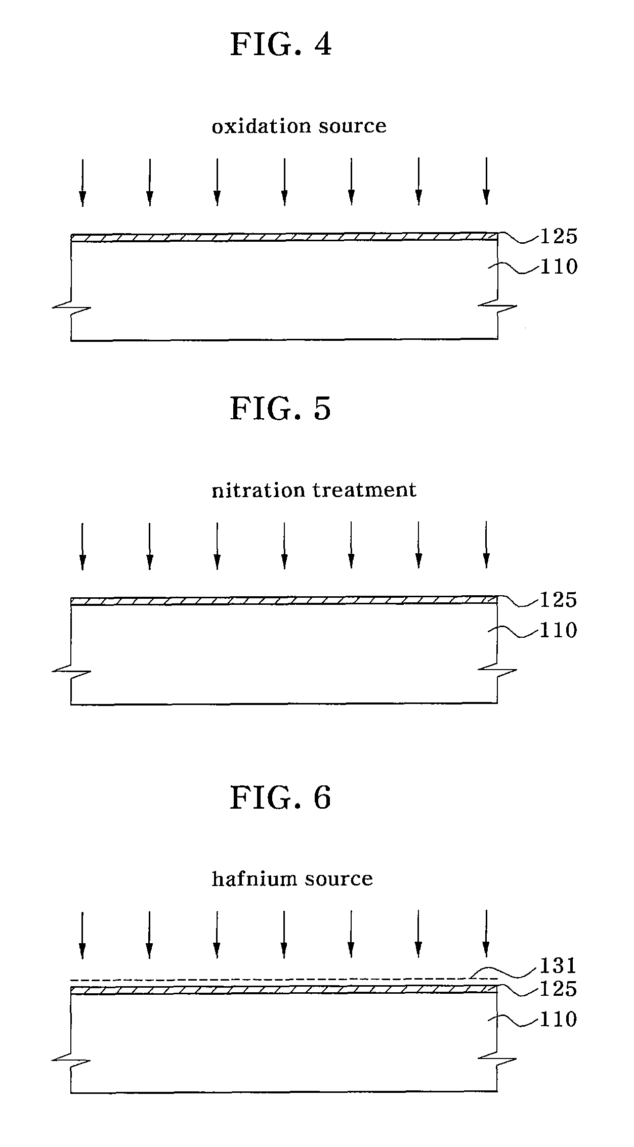
[0043]According to one embodiment of the present invention, a non-volatile memory device and a method for fabricating the device employ a charge trapping structure having a stack consisting of three high-dielectric layers. The charge trapping structure consisting of a charge tunneling layer, a charge trapping layer and a blocking layer prevents formation of a silicon oxidation layer on a surface of a silicon substrate.

[0044]The composition of the three layers may be changed depending on a variation in deposition temperature and composition ratio to provide the constituent layers with different dielectric constants. Thus, a difference in energy band gap between the layers occurs. Accordingly, a charge trap is created via an energy well structure.

[0045]As a result, an undesired increase can be prevented in the thickness of an equivalent oxide film, which is caused by formation of a silicon oxide film on an interface between a silicon semiconductor substrate and a charge tunneling laye...


PUM


Abstract

A method for fabricating a non-volatile memory device includes forming a charge tunneling layer composed of a hafnium silicate (HfSixOyNz) layer on a semiconductor substrate. A charge trapping layer composed of a hafnium oxide nitride (HfOxNy) layer is formed on the charge tunneling layer. A charge blocking layer composed of a hafnium oxide layer is formed on the charge trapping layer. A gate layer is formed on the charge blocking layer. A non-volatile memory device fabricated by the method is also disclosed.

Description

CROSS-REFERENCE TO RELATED APPLICATION[0001]The present application claims priority to Korean patent application number 10-2007-0037030, filed on Apr. 16, 2007, which is incorporated by reference in its entirety.BACKGROUND OF THE INVENTION[0002]The present invention relates to a non-volatile memory device and a method for fabricating the same.[0003]Non-volatile memory devices for performing memory operations in the absence of an electric power have attracted much attention as next-generation semiconductor memory devices. In particular, flash memory devices employing a floating gate are widely utilized in a variety of applications. In addition, metal oxide nitride oxide semiconductor (MONOS) and silicon oxide nitride oxide semiconductor (SONOS) memory devices are being developed.[0004]Floating gate memory devices perform memory operations via potential wells. Flash electrically erasable read only memory (EEPROM), e.g., EPROM tunnel oxide (ETox), is commonly used as a floating gate me...

Claims


Application Information

Patent Timeline
Patent Type & Authority Patents(United States)
IPC IPC(8): H01L21/336
CPCH01L29/66833H01L29/792H01L29/4234
Inventor PARK, CHANG SOO
Owner SK HYNIX INC
Why Eureka
Try Eureka