Formation method of single crystal semiconductor layer, formation method of crystalline semiconductor layer, formation method of polycrystalline layer, and method for manufacturing semiconductor device

a technology of crystalline semiconductor and formation method, which is applied in the field of single crystal semiconductor layer, formation method of crystalline semiconductor layer, formation method of polycrystalline layer, and method for manufacturing semiconductor device, can solve the problem that the entire surface of the glass substrate cannot be covered by one silicon wafer, and it is difficult to closely spread a plurality of silicon wafers over the glass substrate, so as to reduce the constraints on the design rules of the semiconductor device, the effect of poor crystallinity and small variation

Inactive Publication Date: 2011-02-15
SEMICON ENERGY LAB CO LTD
View PDF9 Cites 42 Cited by
  • Summary
  • Abstract
  • Description
  • Claims
  • Application Information

AI Technical Summary

Benefits of technology

[0011]A separation layer is provided concentrically with the top face of the cylindrical single crystal semiconductor ingot or along the side surface thereof, and the cylindrical single crystal semiconductor ingot is separated in the direction perpendicular to the central axis; thus, a single crystal semiconductor layer having large area can be obtained. That is, a single crystal semiconductor layer is separated from the cylindrical single crystal semiconductor ingot like by rotary cutting.
[0013]The present invention makes it possible to form a large single crystal semiconductor layer. Using a large single crystal semiconductor layer obtained in accordance with the present invention, a large semiconductor device using a single crystal semiconductor layer with a little variation as an active layer can be used.
[0014]Since a large single crystal semiconductor layer of the present invention does not have a region with poor crystallinity, there would be no constraints that circuits are necessarily designed to avoid production of a region with a poor crystallinity. Therefore, the constraints on the design rules of the semiconductor device are reduced.
[0015]Further, a large single crystal semiconductor layer can be formed by the present invention, more active layers can be formed from a single crystal semiconductor layer; thus, mass production of semiconductor devices is made possible.

Problems solved by technology

Therefore, the entire surface of the glass substrate cannot be covered by one silicon wafer.
Therefore, although a plurality of silicon wafers are required to be bonded onto the glass substrate, it is difficult to closely spread a plurality of silicon wafers over the glass substrate.
There is no silicon in the space between adjacent silicon wafers, so that there are constraints on circuit design, which greatly reduces latitude in design rules.

Method used


Image

  • Formation method of single crystal semiconductor layer, formation method of crystalline semiconductor layer, formation method of polycrystalline layer, and method for manufacturing semiconductor device
  • Formation method of single crystal semiconductor layer, formation method of crystalline semiconductor layer, formation method of polycrystalline layer, and method for manufacturing semiconductor device
  • Formation method of single crystal semiconductor layer, formation method of crystalline semiconductor layer, formation method of polycrystalline layer, and method for manufacturing semiconductor device

Examples


embodiment modes

[0060]Embodiment modes and embodiments of the present invention will be explained with reference to the drawings. However, the present invention is not limited to the following description. As is readily appreciated by those skilled in the art, the mode and the detail of the present invention can be changed in various ways without departing from the spirit and the scope of the present invention. Therefore, the present invention should not be construed as being limited to the description of the embodiment modes to be given below. Note that in the drawings for illustrating the structures of the invention, like portions are denoted by the same reference numerals throughout the drawings.

[0061]Note that in this specification, “semiconductor device” refer to general devices which can function by utilizing semiconductor properties, and display devices using liquid crystal, electroluminescence (EL), or the like, semiconductor circuits, and electronic devices are all defined as semiconductor...

embodiment mode 1

[0062]This embodiment mode will be described with reference to FIGS. 1A to 1C, FIGS. 2A to 2D, and FIGS. 7A to 7E.

[0063]In this embodiment mode, an example in which a silicon ingot is used as a single crystal semiconductor ingot, and as a single crystal semiconductor layer having large area, a single crystal silicon layer is separated from the silicon ingot and bonded to a large insulating substrate, for example, a large glass substrate, will be described.

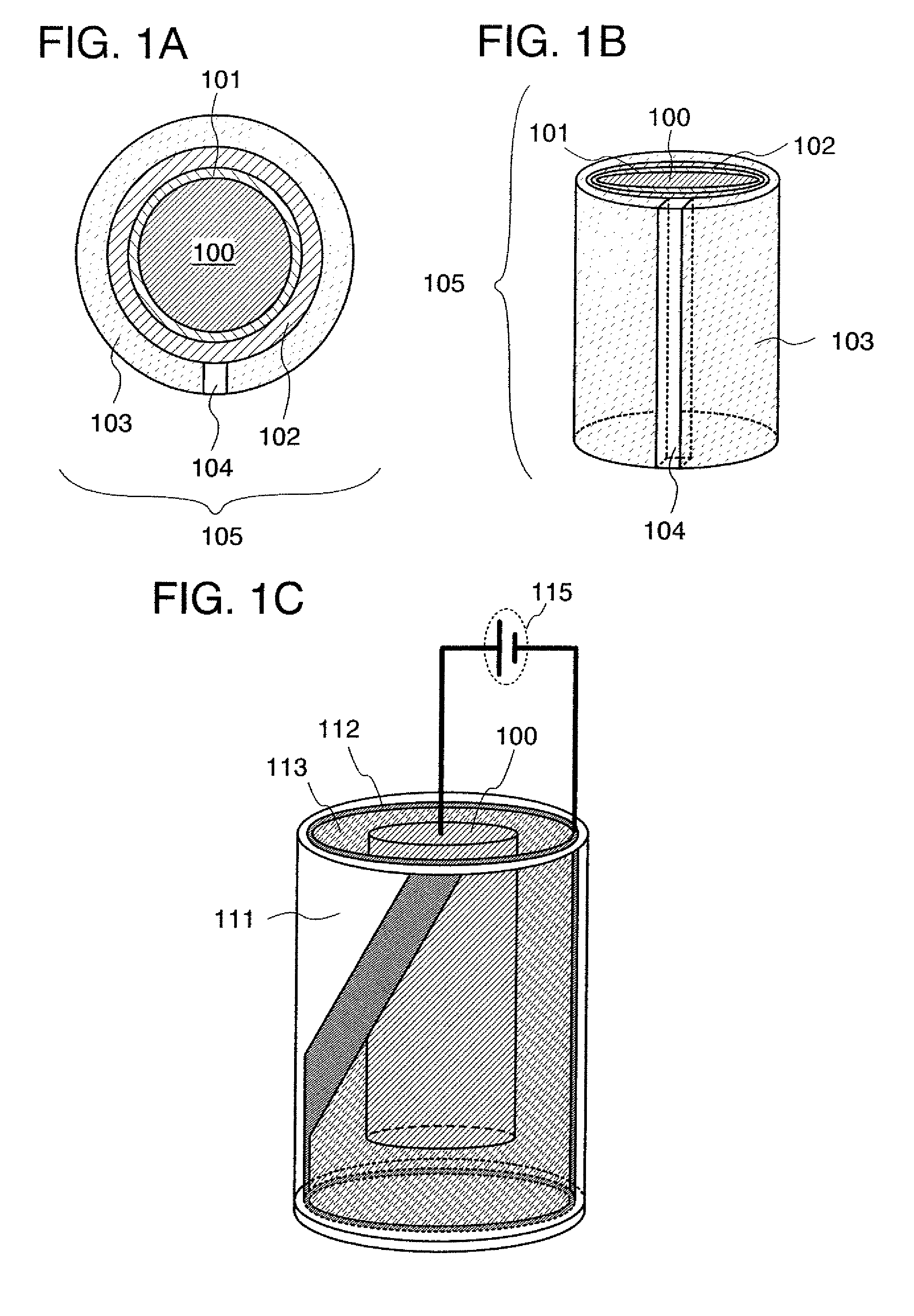
[0064]First, anodization is performed on the entire side surface of a silicon ingot 100, and a first porous silicon layer 101 and a second porous silicon layer 102 are formed as a first porous layer and a second porous layer, respectively. In this embodiment mode, the silicon ingot 100 used has a diameter of 30 cm and a length of 100 cm or more.

[0065]Note that in the present invention, a semiconductor is not limited to silicon, and another semiconductor, for example, germanium, silicon germanium, or the like, and an oxide semicondu...

embodiment mode 2

[0090]In this embodiment mode, a method for obtaining a single crystal silicon layer having large area, which is different from that in Embodiment Mode 1, a method for obtaining a single crystal silicon layer, a method for manufacturing a semiconductor device using the single crystal silicon layer will be described with reference to FIGS. 3A to 3B, FIGS. 4A to 4D, and FIGS. 8A to 8C.

[0091]Further, in this embodiment mode, an example in which a silicon ingot is used as a single crystal semiconductor ingot, and as a single crystal semiconductor layer having large area, a single crystal silicon layer is separated from the silicon ingot and bonded to a large insulating substrate, for example, a large glass substrate, as in Embodiment Mode 1 will be described.

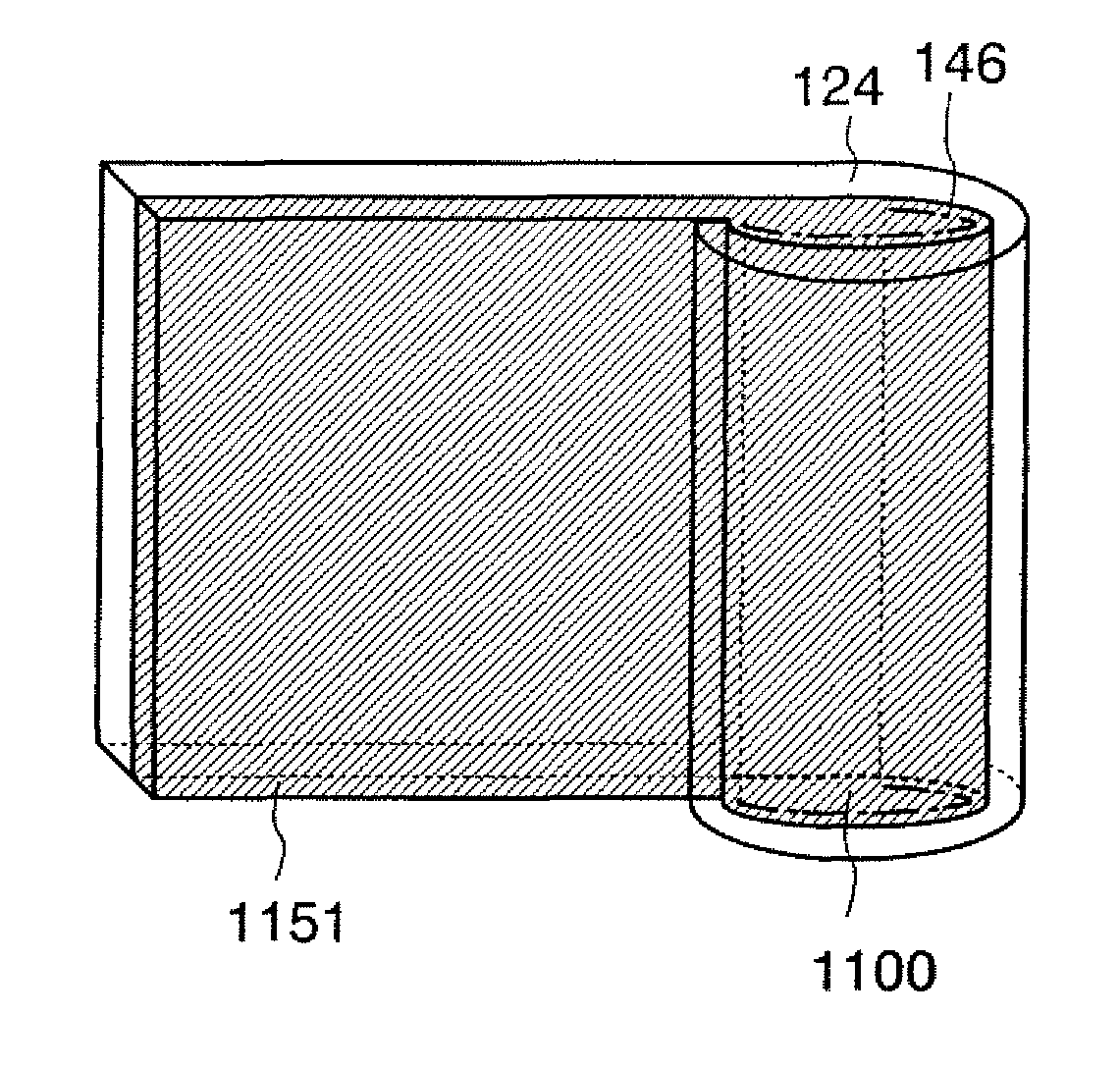
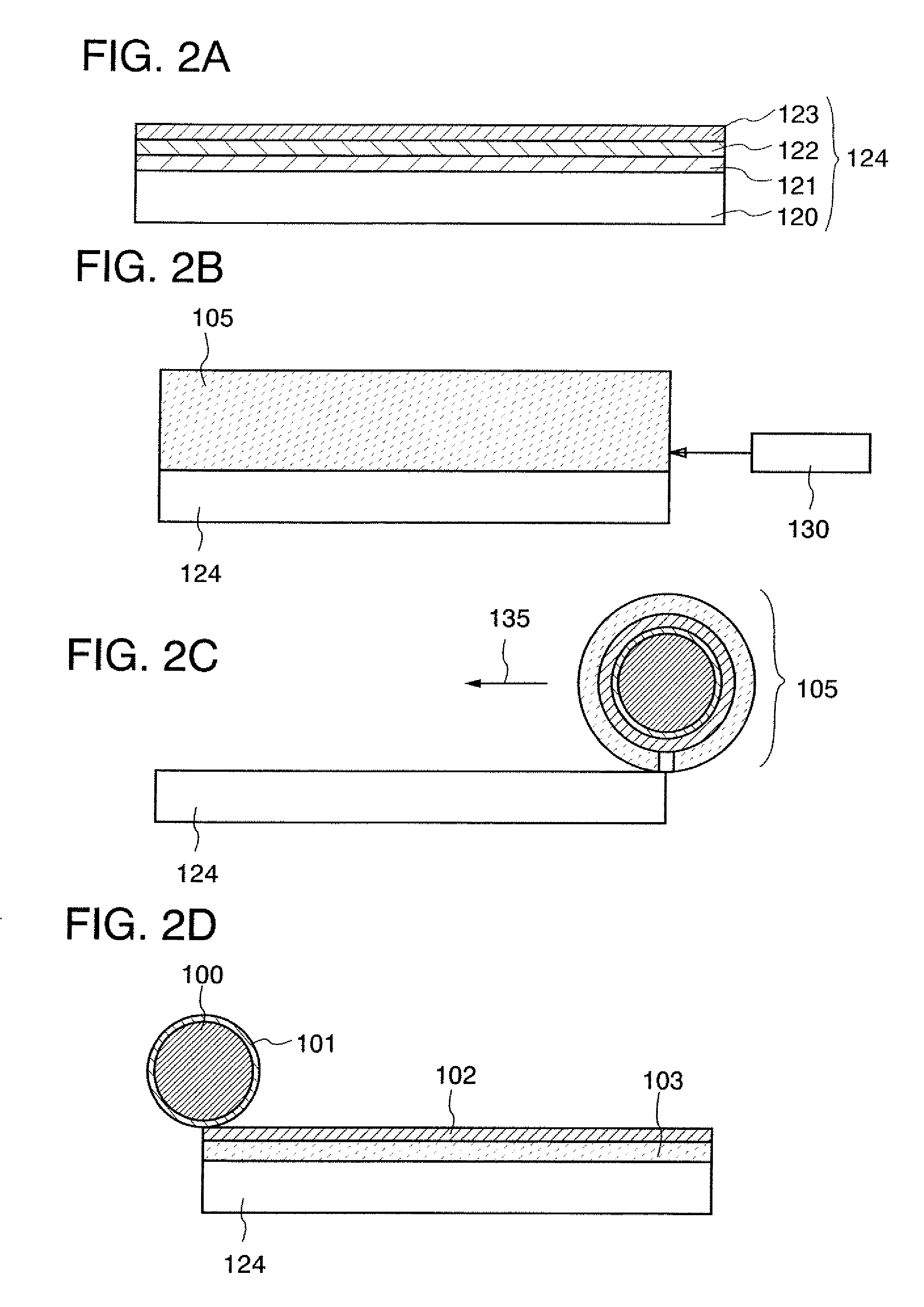
[0092]First, based on Embodiment Mode 1, the substrate 124 in which the first insulating film 121, the second insulating film 122, and the third insulating film 123 are formed over the large insulating substrate 120 is prepared.

[009...


PUM

PropertyMeasurementUnit
sizeaaaaaaaaaa
lengthaaaaaaaaaa
diameteraaaaaaaaaa

Abstract

A method for forming a single crystal semiconductor layer in which a first porous layer and a second porous layer are formed over a single crystal semiconductor ingot, a groove is formed in a part of the second porous layer and a single crystal semiconductor layer is formed over the second porous layer, the single crystal semiconductor ingot is attached onto a large insulating substrate, water jet is directed to the interface between the first porous layer and the second porous layer, and the single crystal semiconductor layer is attached to the large insulating substrate, or a method for forming a crystalline semiconductor layer in which a crystalline semiconductor ingot is irradiated with hydrogen ions to form a hydrogen ion irradiation region in the crystalline semiconductor ingot, the crystalline semiconductor ingot is rolled over the large insulating substrate while being heated, the crystalline semiconductor layer is separated from the hydrogen ion irradiation region, and the crystalline semiconductor layer is attached to the large insulating substrate.

Description

BACKGROUND OF THE INVENTION[0001]1. Field of the Invention[0002]The present invention relates to a substrate having a silicon-on-insulator (SOI) structure obtained by slicing a semiconductor layer from a crystalline semiconductor substrate and bonding it to a substrate of a different kind. In particular, the present invention relates to bonding SOI technology. The present invention relates to a method for manufacturing an SOI substrate in which a single crystal or polycrystalline semiconductor layer is bonded to a substrate having an insulating surface of glass or the like. Further, the present invention relates to a semiconductor device using a substrate that has such an SOI structure and a method for manufacturing such a semiconductor device.[0003]2. Description of the Related Art[0004]Instead of silicon wafers that are manufactured by thinly cutting an ingot of a single crystal semiconductor, semiconductor substrates called silicon-on-insulator (SOI) substrates have been develope...

Claims


Application Information

Patent Timeline
Patent Type & Authority Patents(United States)
IPC IPC(8): H01L21/20H01L21/36
CPCC30B29/06C30B31/22C30B35/00H01L21/76251C30B33/00H01L27/1214H01L27/1266H01L21/76254
Inventor TANAKA, KOICHIROOKAMOTO, SATORU
Owner SEMICON ENERGY LAB CO LTD
Why Eureka
Try Eureka