Organic light emitting device and method for manufacturing the same

a light-emitting device and organic compound technology, applied in the direction of discharge tube/lamp details, discharge tube luminescent compositions etc., can solve the problems of affecting the performance of the device, the instability of the interface between the electrode formed of metal, metal oxides or conductive polymers and the organic compound layer, and the inability to select a material for the hole injection layer, etc., to achieve excellent device performance, efficiency, luminance, or driving voltage

Active Publication Date: 2011-10-18
LG CHEM LTD
View PDF50 Cites 3 Cited by
  • Summary
  • Abstract
  • Description
  • Claims
  • Application Information

AI Technical Summary

Benefits of technology

[0076]As describe above, the organic light emitting device according to the present invention has a low energy barrier for hole injection and excellent charge transport ability of an organic compound layer for charge transport so as to have excellent device performance, such as efficiency, luminance, or a driving voltage. Further, since various materials can be used as a material for an electrode, a device manufacturing process can be simplified. In addition, since the anode and the cathode can be formed of the same material, a layered organic light emitting device having high luminance can be obtained.

Problems solved by technology

However, an interface between the electrode formed of metal, metal oxides, or conductive polymers and the organic compound layer is unstable.
Accordingly, heat applied from the outside, internally generated heat, or an electric field applied to the device has an adverse effect on performance of the device.
However, since the hole injection layer needs to be selected in view of an HOMO energy level of a hole transport layer or a light emitting layer close to the hole injection layer as well as in view of the Fermi energy level of the anode, there is a limitation to select a material for the hole injection layer.
However, a material for the anode is limited.
Meanwhile, it has been known that performance characteristics of a device having multi organic compound layers are affected by transport ability of charge carriers of each organic compound layer.

Method used


Image

  • Organic light emitting device and method for manufacturing the same
  • Organic light emitting device and method for manufacturing the same
  • Organic light emitting device and method for manufacturing the same

Examples


example

Example 1

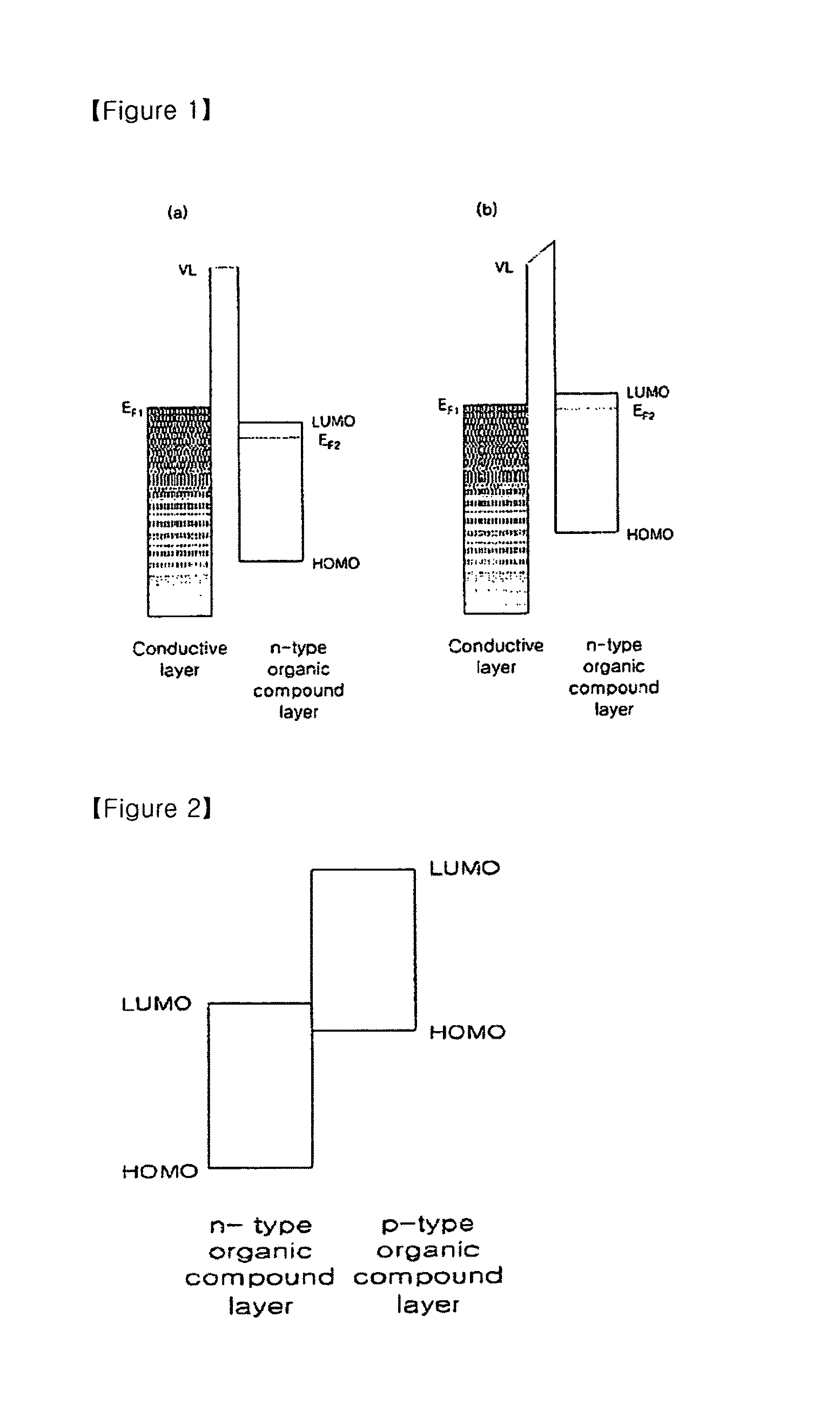
[0094]Measurement of HOMO and LUMO Energy Levels of HAT using UPS and UV-VIS Absorption Methods

[0095]Hexanitrile hexaazatriphenylene (HAT) was used as the organic material having n-type semiconductor characteristics. In order to measure the HOMO level of HAT, a UPS (Ultraviolet photoelectron spectroscopy) method was used. In the method, kinetic energy of electrons that are discharged from a sample when vacuum UV rays (21.20 eV) emitted from the He lamp are radiated onto the sample in a ultravacuum (0 to 8 torr) is analyzed to detect a work function of metal, or to detect ionization energy of organic material, that is, the HOMO level and the Fermi energy level. That is, the kinetic energy of electrons that are discharged from the sample when the vacuum UV rays (21.20 eV) are radiated onto the sample is a difference between 21.2 eV that is vacuum UV energy and electron binding energy of the sample to be measured. Accordingly, a binding energy distribution of molecules in the...

example 2

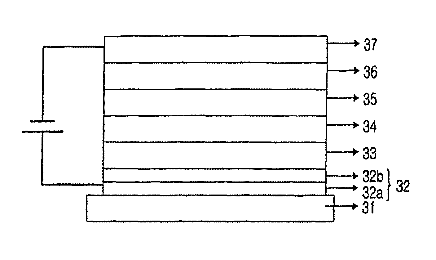
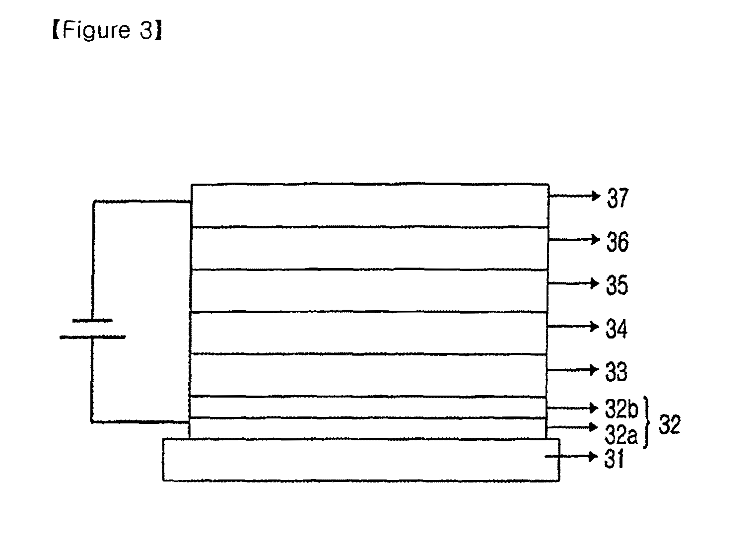
[0099]A glass substrate (Corning 7059 glass) on which an ITO (indium tin oxide) was applied to a thickness of 1000 Å was put in distilled water where a detergent (Manufacturing company: Fischer Co., and Product No.: 15-335-55) was dissolved to perform washing using ultrasonic waves for 30 min. Subsequently, the glass substrate was put in distilled water to repeat ultrasonic washing for 5 min twice.

[0100]Once the distilled water washing was finished, the glass substrate was subjected to ultrasonic washing sequentially using isopropyl alcohol, acetone, and methanol solvents one by one, and then dried. Subsequently, the glass substrate on which ITO was applied was subjected to plasma treatment using a nitrogen plasma in the plasma washing machine at pressure of 14 mtorr under powder condition of 50 W for 5 min. The work function of the surface treated ITO anode was about 4.8 eV.

[0101]Subsequently, the glass substrate on which ITO was applied was subjected to plasma treatment using an o...


PUM


Abstract

Disclosed is an organic light emitting device and a method for manufacturing the same. The organic light emitting device includes a first electrode, one or more organic compound layers, and a second electrode. The first electrode includes a conductive layer and an n-type organic compound layer disposed on the conductive layer. A difference in energy between an LUMO energy level of the n-type organic compound layer of the first electrode and a Fermi energy level of the conductive layer of the first electrode is 4 eV or less. One of the organic compound layers interposed between the n-type organic compound layer of the first electrode and the second electrode is a p-type organic compound layer forming an NP junction along with the n-type organic compound layer of the first electrode. A difference in energy between the LUMO energy level of the n-type organic compound layer of the first electrode and an HOMO energy level of the p-type organic compound layer is 1 eV or less. One or more layers interposed between the conductive layer of the first electrode and the second electrode is n-doped or p-doped with an organic material or an inorganic material.

Description

[0001]This application claims the benefit of the filing date of Korean Patent Application No. 10-2005-0064430 filed on Jul. 15, 2005 in the Korean Intellectual Property Office and International Application PCT / KR2006 / 002768 filed Jul. 14, 2006, both of which are incorporated herein in its entirety by reference.TECHNICAL FIELD[0002]The present invention relates to an organic light emitting device that has a low energy barrier for hole injection from an electrode to an organic compound layer, a low driving voltage, and high efficiency and luminance, and to a method for manufacturing the organic light emitting device. Specifically, the present invention relates to an organic light emitting device, in which an n-type organic compound layer is formed in a hole injection electrode, and at least one layer of organic compound layers is n-doped or p-doped with an organic or inorganic material, and a method for manufacturing the organic light emitting device. This application claims the benef...

Claims


Application Information

Patent Timeline
Patent Type & Authority Patents(United States)
IPC IPC(8): H01J1/62H01J63/04
CPCH01L51/5088H01L51/5278H10K50/17H10K50/19H05B33/26C09K11/06H05B33/10
Inventor KANG, MIN SOOSON, SE HWANCHOI, HYEON
Owner LG CHEM LTD
Why Eureka
Try Eureka