Method for forming an interfacial passivation layer on the Ge semiconductor

a technology of interfacial passivation and germanium semiconductor, which is applied in the direction of semiconductor/solid-state device manufacturing, basic electric elements, electric apparatus, etc., can solve the problems of gate leakage current increasing, threshold voltage shift, and inability to form interfaces, etc., to achieve great innovation and advancement, good quality

Active Publication Date: 2011-12-06
NAT CHIAO TUNG UNIV
View PDF0 Cites 10 Cited by
  • Summary
  • Abstract
  • Description
  • Claims
  • Application Information

AI Technical Summary

Benefits of technology

[0020]Due to the invention can form an interfacial passivation layer with good quality under low-temperature process of 150° C., thus the development of technology has great innovation and advancement.
[0021]Therefore, the advantage and spirit of the invention can be understood further by the following detail description of invention and attached Figures.

Problems solved by technology

However, large density of state contained between the high-k dielectric and germanium channel, and diffusion of germanium in high-k dielectric during inevitable thermal process, result in threshold voltage shift and gate leakage current increasing.
Thus, the interface is unable to be formed after the gate insulator deposition, and the defect generation in gate insulator could occur again during sequent thermal process.
The process temperature could be too high, and the interface is unable to be formed after the gate insulator deposition, and the defects could generate in gate insulator during sequent thermal process
The interface is unable to be formed after the gate insulator deposition, and the defects could generate in gate insulator during sequent thermal process.
It will always cause the significant thermal diffusion of germanium and the surface damage of germanium.
The poor thermal stability of germanium oxide cause chemical reaction of germanium oxide and germanium substrate.
Sequent thermal decomposition of germanium oxide results poor interface between gate dielectric and germanium substrate, and thermal diffusion of germanium in gate dielectric.

Method used


Image

  • Method for forming an interfacial passivation layer on the Ge semiconductor
  • Method for forming an interfacial passivation layer on the Ge semiconductor
  • Method for forming an interfacial passivation layer on the Ge semiconductor

Examples


first embodiment

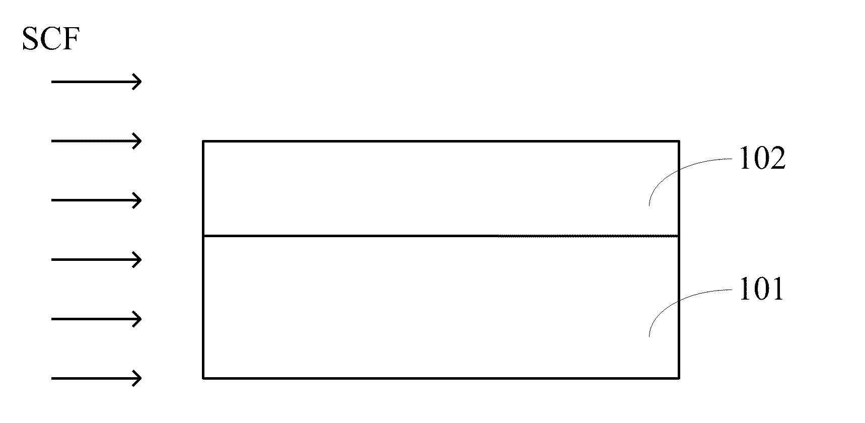
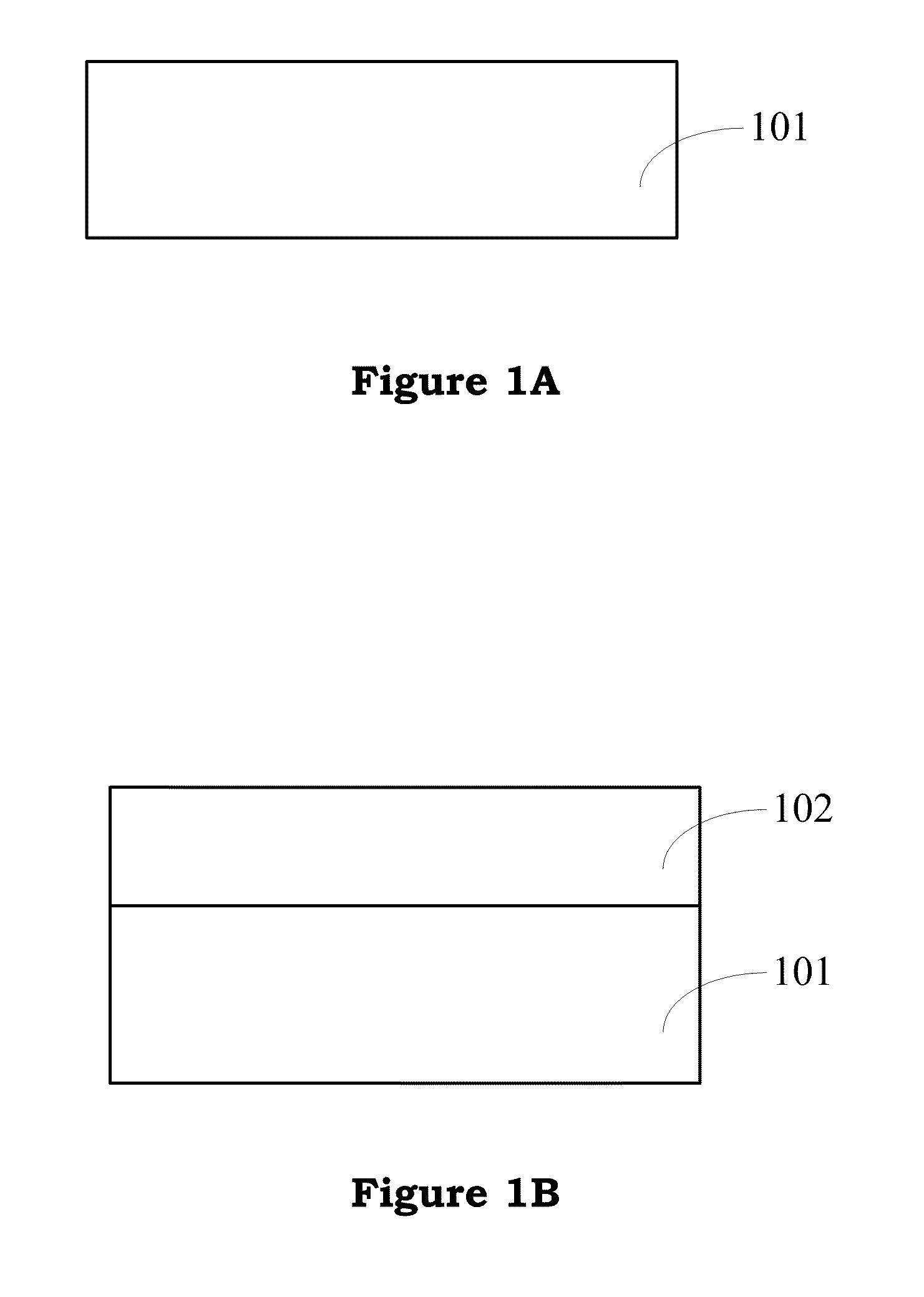
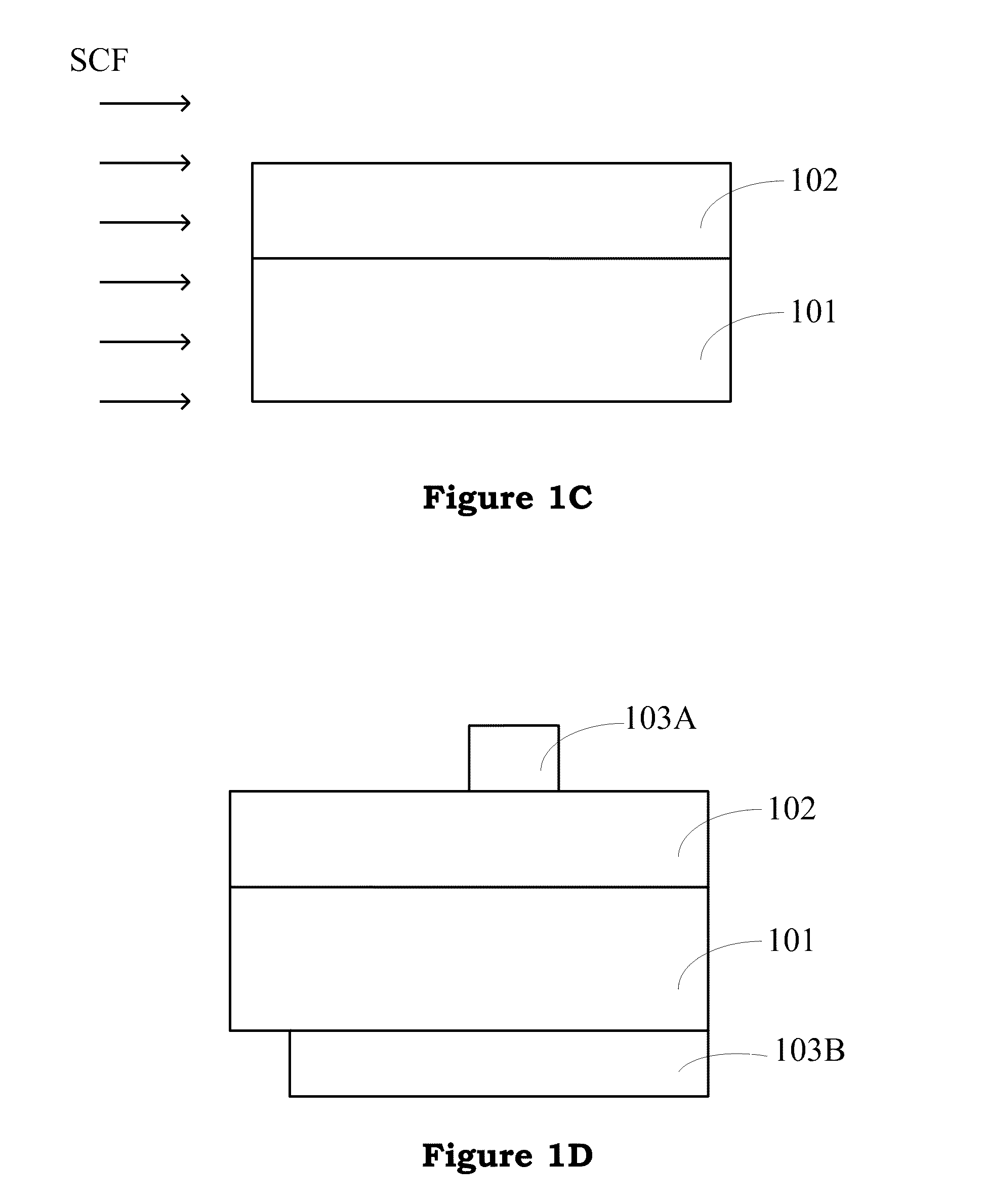
[0030]The invention relates to a method for forming an interfacial passivation layer on the germanium (Ge) semiconductor. The detail of FIG. 1A to FIG. 1D in the first embodiment is described as follows:

[0031]As shown in FIG. 1A, firstly, the general epitaxy technology (such as Molecular Beam Epitaxy process, Metal-Organic Chemical Vapor Deposition process) is employed to deposit a Ge semiconductor layer 101 (about 2.5 μm thick).

[0032]As shown in FIG. 1B, the Low Pressure Chemical Vapor Deposition System (LPCVD) is employed to deposit a silicon dioxide (SiO2) layer 102 (about 12 nm thick) on the Ge semiconductor layer 101 (including P-type Ge semiconductor layer or N-type Ge semiconductor layer), which is used as the gate insulator layer.

[0033]As shown in FIG. 1C, mix the carbon dioxide gas, 1˜10 vol % water oxidant, and propyl alcohol at 100° C. to 200° C. and 1000 psi to 3500 psi to form the low-temperature supercritical fluid (SF). Carry the supercritical fluid into the interface...

second embodiment

[0035]The invention relates to a method for forming an interfacial passivation layer on the Ge semiconductor after thermal annealing. The detail of FIG. 2A to FIG. 2E in the second embodiment is described as follows:

[0036]As shown in FIG. 2A, firstly, the general epitaxy technology (such as Molecular Beam Epitaxy process, Metal-Organic Chemical Vapor Deposition process) is employed to deposit a Ge semiconductor layer 201 (about 2.5 u, thick).

[0037]As shown in FIG. 2B, the Low Pressure Chemical Vapor Deposition System (LPCVD) is employed to deposit a silicon dioxide (SiO2) layer 202 (about 12 nm thick) on the Ge semiconductor layer 201 (including P-type Ge semiconductor layer or N-type Ge semiconductor layer), which is used as the gate insulator layer.

[0038]As shown in FIG. 2C, the annealing treatment is performed for the silicon dioxide layer (insulator layer) 202 and the Ge semiconductor layer 201 at about 400° C.

[0039]As shown in FIG. 2D, mix the carbon dioxide gas, 1˜10 vol % wat...


PUM

PropertyMeasurementUnit
thicknessaaaaaaaaaa
temperatureaaaaaaaaaa

Abstract

The invention discloses a method for forming an interfacial passivation layer on the Ge semiconductor. The supercritical CO2 fluids is used to form an interfacial passivation layer between Ge channel and gate insulator layer, and improve the dielectric characteristics of gate insulator after high-temperature thermal annealing process.

Description

BACKGROUND OF THE INVENTION[0001]1. Field of the Invention[0002]The invention relates to a method for forming a protection layer on the semiconductor, particularly to a method for forming an interfacial passivation layer on the germanium semiconductor.[0003]2. Description of the Prior Art[0004]At present, the development trend for the manufacturing technology of the integrated circuit (IC) is still kept to the trend of miniaturizing transistor size, in order to reach the goal of high efficacy and high density. Due to the efficacy of conventional polycrystalline silicon / silicon dioxide / silicon channel metal-oxide-semiconductor field effect transistor is unable to be increased by the miniaturizing technology, thus, how to increase the mobility of carrier and the dielectric capacitance of gate has become the key technology and goal for the development of field effect transistor in the next generation. Wherein, the mobility for the electron and hole of Ge semiconductor is 2 times and 4 ...

Claims


Application Information

Patent Timeline
Patent Type & Authority Patents(United States)
IPC IPC(8): H01L21/02
CPCH01L21/02164H01L21/02343H01L21/28255
Inventor LIU, PO-TSUNHUANG, CHEN-SHUOHUANG, YI-LINGCHENG, SZU-LINSZE, SIMON M.NISHI, YOSHIO
Owner NAT CHIAO TUNG UNIV
Why Eureka
Try Eureka