

Two stage plasma etching method for enhancement mode GaN HFET
- Summary
- Abstract
- Description
- Claims
- Application Information
AI Technical Summary
Benefits of technology
Problems solved by technology
Method used
Image

Examples
Embodiment Construction
[0035]In the following detailed description, only certain exemplary embodiments of the present invention are shown and described, by way of illustration. As those skilled in the art would recognize, the described exemplary embodiments may be modified in various ways, all without departing from the spirit or scope of the present invention. Accordingly, the drawings and description are to be regarded as illustrative in nature, and not restrictive.
[0036]While the invention has been described in connection with certain exemplary embodiments, it is to be understood by those skilled in the art that the invention is not limited to the disclosed embodiments, but, on the contrary, is intended to cover various modifications included within the spirit and scope of the appended claims and equivalents thereof.
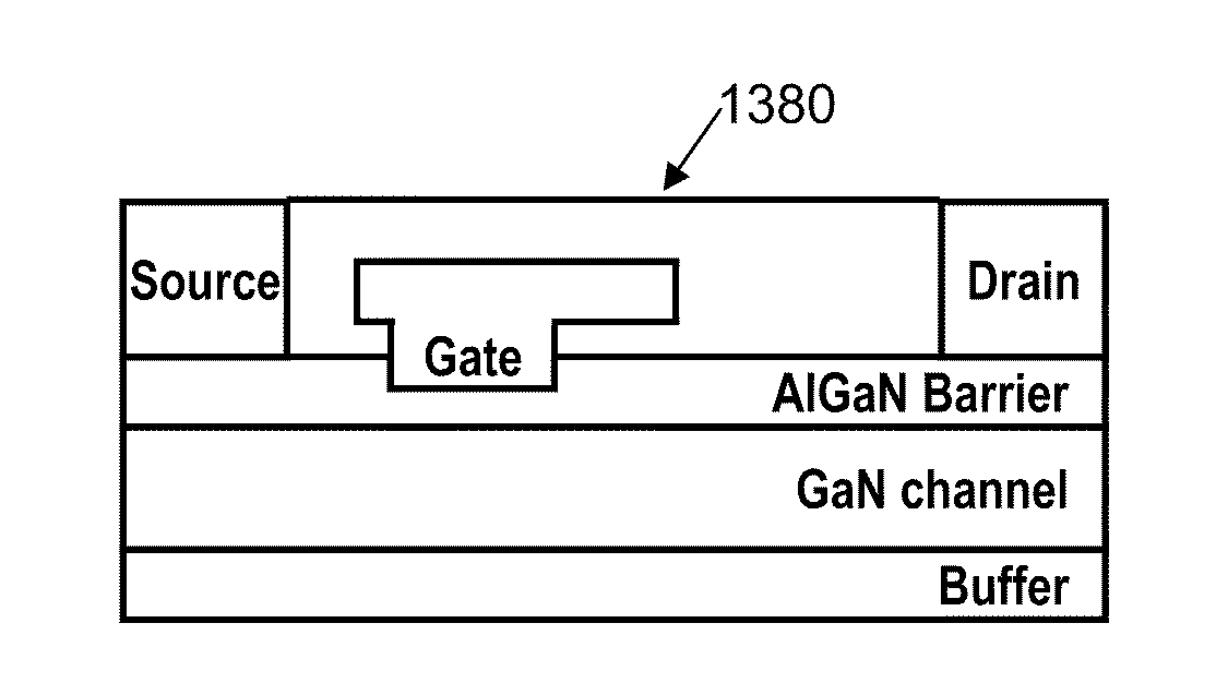
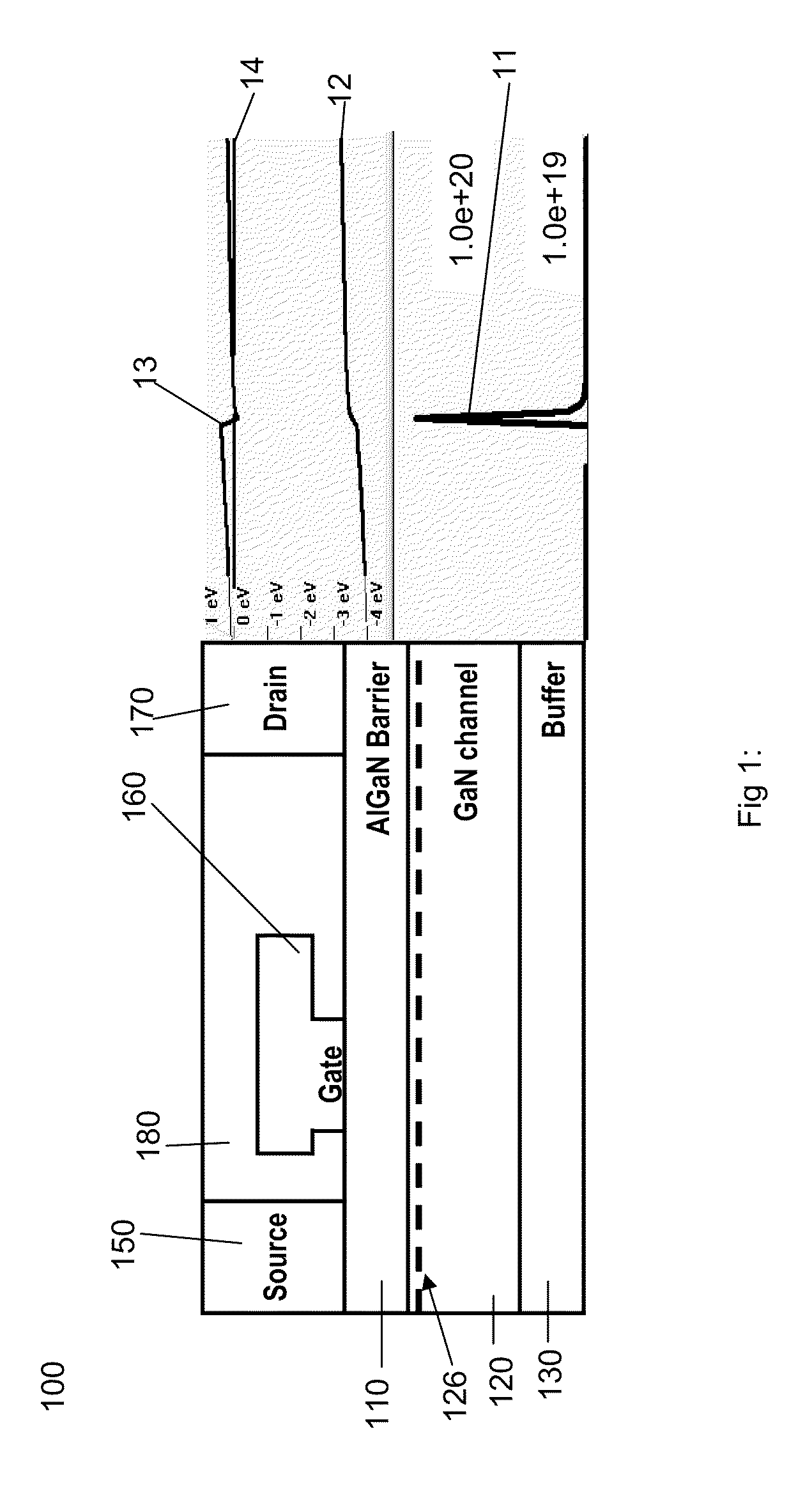
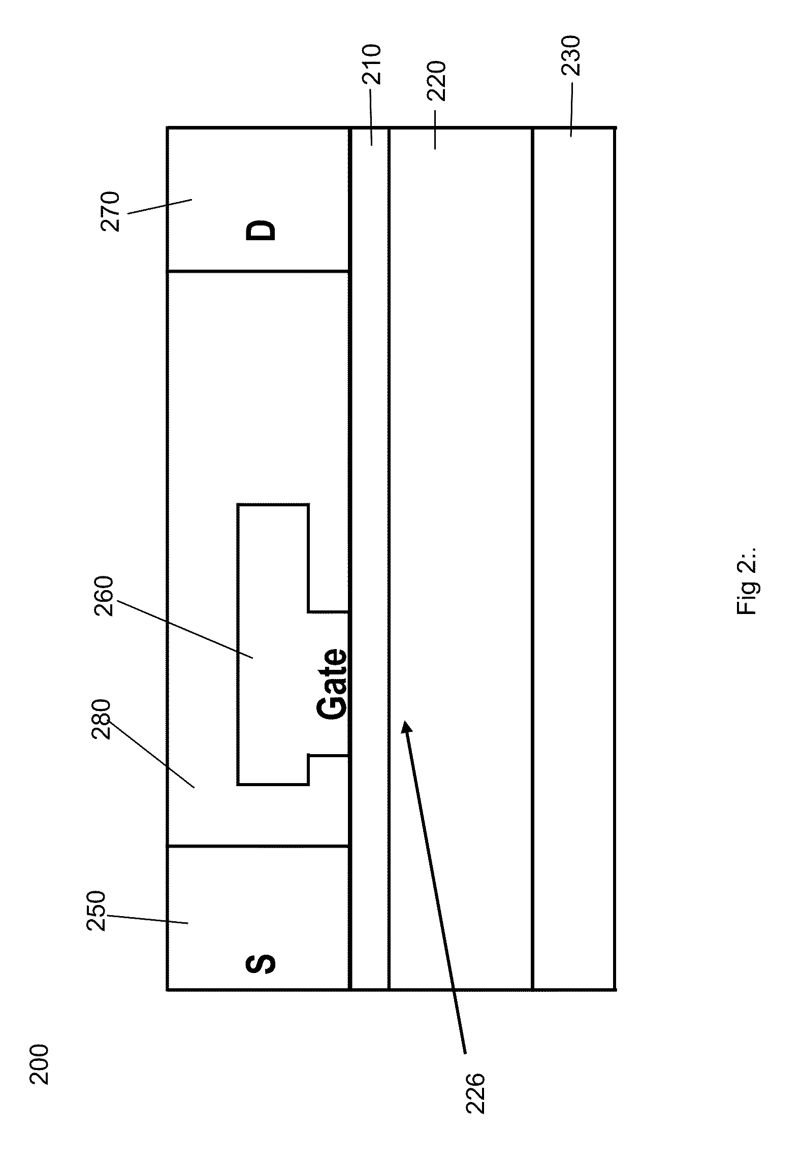
[0037]A thin-grown AlGaN barrier layer is undesirable because of the inability to conduct from source to drain. Fluorine-treatment is undesirable because of non-uniformity, implant damage a...
PUM
 Abstract
Description
Claims
Application Information