Scanning probe microscope and sample observing method using the same

a scanning probe and microscope technology, applied in the direction of instruments, surface/boundary effects, measurement devices, etc., can solve the problems of atomic force microscopes not measuring optical properties, spatial resolution coming short in general raman spectroscopic micrometers, and limit in classifying performance, etc., to achieve high repeatability, improve defect classifying performance, and high yield ratio

Active Publication Date: 2012-09-18
HITACHI LTD
View PDF14 Cites 4 Cited by
  • Summary
  • Abstract
  • Description
  • Claims
  • Application Information

AI Technical Summary

Benefits of technology

[0022]In accordance with the present invention, it is possible to measure the optical information and the surface profile information of the sample surface at a nanometer order resolution and at a high repeatability without damaging both the probe and the sample. As a result, since it is possible to measure the physical information such as the stress distribution, the impurity distribution and the like of the semiconductor sample, and it is possible to measure the optical information and the surface profile information contributing to the classification of the foreign particle and the defect, a foreign particle and defect classifying performance is improved. Further, there can be obtained an effect that a semiconductor device can be produced at a high yield ratio with a high reliability by feeding back the result of measurement to the semiconductor manufacturing process condition.

Problems solved by technology

However, the atomic force microscope can not measure an optical property such as a reflectivity distribution and a refractive index distribution of a sample surface.
An optical method such as a Raman spectrometer measuring method and the like has been under review, however, a spatial resolution comes short in a general Raman spectroscopic micrometer.
Further, in order to specify a generation factor of a foreign particle and a defect detected by a foreign particle inspection and a defect inspection, a classifying work of the foreign particle and the defect is carried out by an electron microscope called as a review SEM, however, since it is a method depending only on a shape and a surface profile information, there is a limit in a classifying performance.
In this case, it is possible to expect an improvement of the classifying performance by adding the optical information, however, the spatial resolution still comes short in the general optical microscope and laser scanning microscope.

Method used


Image

  • Scanning probe microscope and sample observing method using the same
  • Scanning probe microscope and sample observing method using the same
  • Scanning probe microscope and sample observing method using the same

Examples


embodiment 1

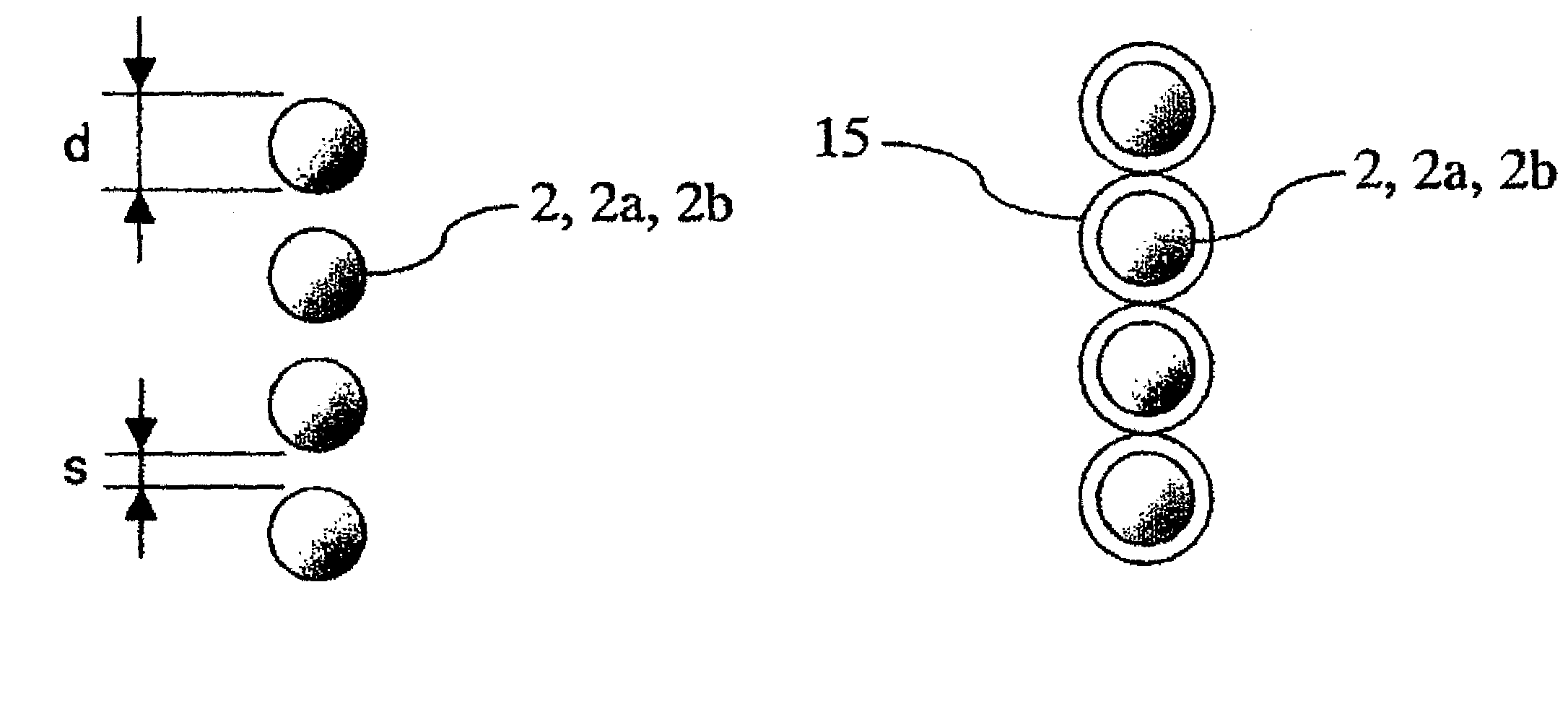
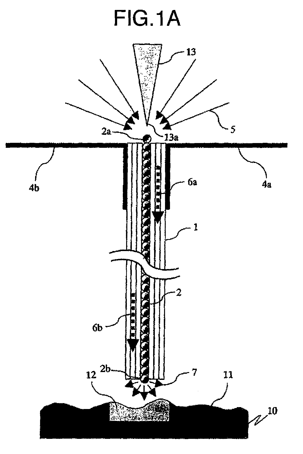
[0026]A description will be given of a first embodiment in accordance with the present invention with reference to FIGS. 1, 2 and 8 to 11. In the present embodiment, as shown in FIG. 1, a plasmon enhanced near field probe is constructed by filling a spherical nano particle 2 of Au in an internal cavity portion of a multi-layer construction carbon nanotube (CNT) provided with a nature serving as a semiconductor or a boron nitride (BN) nanotube 1 exhibiting a nature serving as an insulating material. A filling method can make the inner portion of the nanotube 1 include the gold nano particle 2, for example, by putting the nanotube 1 in which both ends are opened by applying a high tension current or heating and the gold nano particle 2 within a vacuum chamber, carrying out a heating reaction and applying a capillary phenomenon. With regard to the application of the capillary phenomenon, for example, it is possible to apply such a technique as to be disclosed as (http: / / www1.accsnet.ne...

embodiment 2

[0071]A description will be given of a second embodiment in accordance with the present invention with reference to FIGS. 5A and 16. FIG. 5A shows a structure of a plasmon enhanced near field probe in accordance with the present embodiment. A material of the nanotube is a multilayer construction carbon nanotube 40 provided with a nature serving as a semiconductor, in the same manner as the first embodiment, or a boron nitride nanotube 40 exhibiting a nature serving as an insulating material. In the first embodiment and its modified embodiments, the nanotube in which both ends are opened is used, however, the present embodiment used the nanotube 40 in which both ends are closed, and a gold nano particle 2b is fixed to a lower end portion in accordance with a chemical modification or the like. If laser lights 50a and 50b having a wavelength 780 nm are irradiated in a state in which the nanotube 40 is moved down and the gold nano particle 2b is moved close to the sample 10, the gold na...

embodiment 3

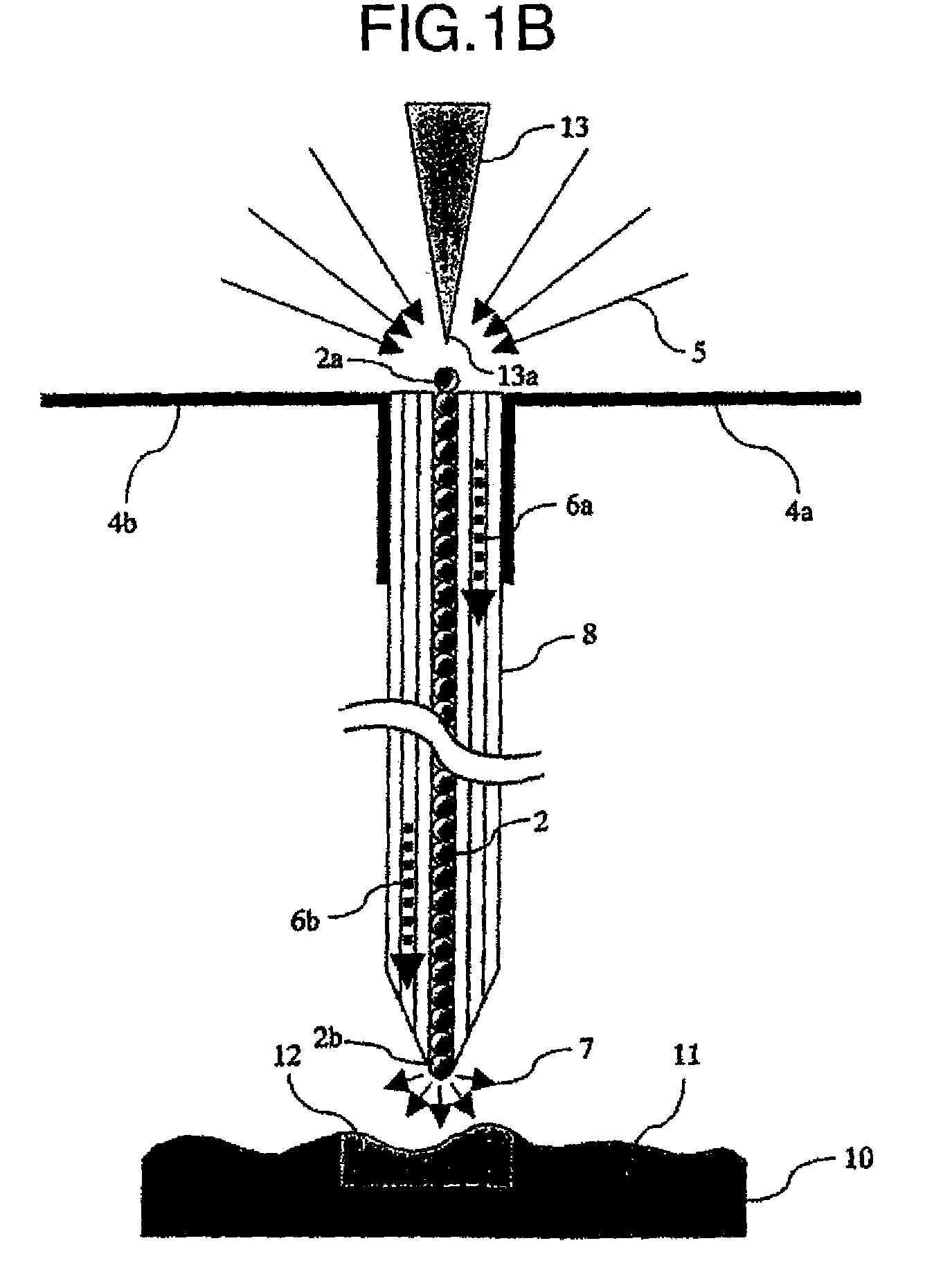
[0083]A description will be given of a third embodiment in accordance with the present invention with reference to FIGS. 7 and 17. FIG. 7 shows a structure of a plasmon enhanced near field probe in the present embodiment. A material of the nano tube is a multilayer construction carbon nanotube 8 provided with a nature serving as the semiconductor in the same manner as the embodiment shown in FIG. 31B, or a boron nitride nanotube 8 exhibiting a nature serving as an insulating material. Further, its structure is absolutely the same as the structure shown in FIG. 31B.

[0084]FIG. 17 shows a structure of a scanning probe microscope mounting the present probe therein. Since the other structures and functions than the optical system are the same as the scanning probe microscope in the first embodiment shown in FIG. 8, a description thereof will be omitted. The light emitted from a semiconductor laser 300 having a wavelength 780 nm is divided into two sections by a beam splitter 302 having a...


PUM

PropertyMeasurementUnit
lengthaaaaaaaaaa
inner diameteraaaaaaaaaa
diameteraaaaaaaaaa

Abstract

In a near-field scanning microscope using an aperture probe, the upper limit of the aperture formation is at most several ten nm in practice. In a near-field scanning microscope using a scatter probe, the resolution ability is limited to at most several ten nm because of the external illuminating light serving as background noise. Moreover, measurement reproducibility is seriously lowered by a damage or abrasion of a probe. Optical data and unevenness data of the surface of a sample can be measured at a nm-order resolution ability and a high reproducibility while damaging neither the probe nor the sample by fabricating a plasmon-enhanced near-field probe having a nm-order optical resolution ability by combining a nm-order cylindrical structure with nm-order microparticles and repeatedly moving the probe toward the sample and away therefrom at a low contact force at individual measurement points on the sample.

Description

CROSS REFERENCE TO RELATED APPLICATIONS[0001]The present application claims priority to Japanese Patent Application No. 2007-061201 filed on Mar. 12, 2007 and Japanese Patent Application No. 2007-322722 filed on Dec. 14, 2007, and the entire contents of which are incorporated herein by reference.TECHNICAL FIELD[0002]The present invention relates to a scanning probe microscope technique and a sample observing method using the same.BACKGROUND ART[0003]A scanning probe microscope (SPM) has been known as a measuring technique of a micro stereoscopic shape. In this technique, an atomic force microscope (AFM) is an observing technique of scanning a sample surface while keeping a contact force to a very small value by controlling an acuate probe, and has been widely used as a technique which can measure an atomic order micro stereoscopic shape. However, the atomic force microscope can not measure an optical property such as a reflectivity distribution and a refractive index distribution of...

Claims


Application Information

Patent Timeline
Patent Type & Authority Patents(United States)
IPC IPC(8): G01N13/00G01B11/30G01Q60/22G01Q70/12
CPCG01Q60/18G01Q60/22B82Y20/00B82Y35/00
Inventor NAKATA, TOSHIHIKOWATANABE, MASAHIROINOUE, TAKASHIHIDAKA, KISHIOHIROOKA, MOTOYUKI
Owner HITACHI LTD
Why Eureka
Try Eureka