Method of making a semiconductor chip assembly with a bump/base/ledge heat spreader, dual adhesives and a cavity in the bump

a semiconductor chip and heat spreader technology, applied in the manufacture of printed circuits, printed circuit aspects, basic electric elements, etc., can solve the problems of heat not only degrading the chip, short life span and immediate failure of the semiconductor device, and high operating temperature, and achieve excellent heat spreading and heat dissipation, low cost, and low thermal conductivity.

Inactive Publication Date: 2013-01-15
BRIDGE SEMICON
View PDF85 Cites 0 Cited by
  • Summary
  • Abstract
  • Description
  • Claims
  • Application Information

AI Technical Summary

Benefits of technology

[0037]The first adhesive can contact the bump and the first dielectric layer in a gap in the first aperture between the bump and the first substrate and contact the base, the ledge and the first dielectric layer outside the gap. The first adhesive can also contact and be sandwiched between the bump and the first dielectric layer, between the ledge and the first dielectric layer and between the base and the ledge. The first adhesive can also be spaced from the second adhesive and the second dielectric layer. The first adhesive can also cover the base outside the bump in the first vertical direction, cover the first substrate in the first vertical direction and cover and surround a sidewall of the bump in the lateral directions. The first adhesive can also conformally coat the sidewall of the bump, a surface of the first dielectric layer that faces in the first vertical direction and a surface of the ledge that faces in the second vertical direction. The first adhesive can also fill the space between the bump and the first substrate and between the ledge and the first substrate. The first adhesive can also extend through the first aperture, extend across the first dielectric layer in the gap and fill the gap. The first adhesive can also be a solidified prepreg with cured epoxy.
[0076]Providing the conductive trace can include providing the pad, the terminal and a plated through-hole that extends through the ledge, the adhesives, the dielectric layers and the conductive layers in an electrically conductive path between the conductive layers. This can include drilling a hole through the ledge, the adhesives, the dielectric layers and the conductive layers, then depositing the plated layer on the conductive layers and in the hole to form a first plated layer on the first conductive layer, a second plated layer on the second conductive layer and the plated through-hole in the hole, then removing selected portions of the first conductive layer and the first plated layer using a first etch mask that defines the pad and removing selected portions of the second conductive layer and the second plated layer using a second etch mask that defines the terminal. In this manner, the conductive trace can provide vertical signal routing between the pad and the terminal.
[0081]The present invention has numerous advantages. The heat spreader can provide excellent heat spreading and heat dissipation without heat flow through the adhesives or the dielectric layers. As a result, the adhesives and the dielectric layers can be a low cost dielectric with low thermal conductivity and not prone to delamination. The first adhesive can be sandwiched between the bump and the first substrate and between the ledge and the first substrate, thereby providing a robust mechanical bond between the heat spreader and the first substrate. The second adhesive can be sandwiched between the ledge and the second substrate, thereby providing a robust mechanical bond between the heat spreader and the second substrate. The heat spreader can have a large surface area with relatively thin metal, thereby reducing weight and cost. The bump and the cavity can be defined by mechanical stamping, thereby enhancing precision. The bump and the ledge can be integral with one another, thereby enhancing reliability. The bump can be customized for the semiconductor device, thereby enhancing the thermal connection. The bump can also have a tapered sidewall and a highly reflective surface layer. As a result, the bump can reflect the light generated by an LED chip mounted on the bump within the cavity, thereby focusing the light in the first vertical direction and enhancing the light output. Furthermore, the cavity can provide a well-defined space for a color-shifting encapsulant deposited on the LED chip. As a result, the color-shifting encapsulant can be dispensed into the cavity in a small consistent amount, thereby enhancing optical performance and reducing cost. The ledge can provide mechanical support for the substrates, thereby preventing warping. The pad and the terminal can include a selected portion of the second conductive layer laminated to the second dielectric layer, thereby enhancing reliability. The conductive trace can provide signal routing with simple circuitry patterns or flexible multi-layer signal routing with complex circuitry patterns. The conductive trace can also provide vertical signal routing between the pad and the terminal using a plated through-hole that extends through the ledge, the adhesives and the dielectric layers to the terminal. The assembly can be manufactured using low temperature processes which reduces stress and improves reliability. The assembly can also be manufactured using well-controlled processes which can be easily implemented by circuit board, lead frame and tape manufacturers.

Problems solved by technology

Semiconductor devices are susceptible to performance degradation as well as short life span and immediate failure at high operating temperatures.
The heat not only degrades the chip, but also imposes thermal stress on the chip and surrounding elements due to thermal expansion mismatch.
LEDs include high power chips that generate high light output and considerable heat.
Unfortunately, LEDs exhibit color shifts and low light output as well as short lifetimes and immediate failure at high operating temperatures.
Furthermore, LED light output and reliability are constrained by heat dissipation limits.
However, since the plastic and the dielectric layer typically have low thermal conductivity, the PBGA provides poor heat dissipation.
However, since the lead frame type interposer has limited routing capability, the QFN package cannot accommodate high input / output (I / O) chips or passive elements.
However, manually dropping the heat slug into the central opening is prohibitively cumbersome and expensive for high volume manufacture.
Furthermore, since the heat slug is difficult to accurately position in the central opening due to tight lateral placement tolerance, voids and inconsistent bond lines arise between the substrate and the heat slug.
The substrate is therefore partially attached to the heat slug, fragile due to inadequate support by the heat slug and prone to delamination.
The heat slug is therefore non-planar and difficult to bond to.
As a result, the assembly suffers from high yield loss, poor reliability and excessive cost.
However, the insulating layer sandwiched between the metal core layer and the PCB limits the heat flow to the PCB.
As a result, the heat spreader releases the heat by thermal convection rather than thermal conduction which severely limits the heat dissipation.
Consequently, the substrate is unbalanced and wobbles and warps during manufacture.
This creates enormous difficulties with chip mounting, wire bonding and encapsulant molding.
Furthermore, the expanded base may be bent by the encapsulant molding and may impede soldering the package to the next level assembly as the solder balls collapse.
As a result, the package suffers from high yield loss, poor reliability and excessive cost.
However, the electrical contacts are difficult to mount on the insulating layer, difficult to electrically connect to the next level assembly and fail to provide multi-layer routing.
Conventional packages and thermal boards thus have major deficiencies.
For instance, dielectrics with low thermal conductivity such as epoxy limit heat dissipation, whereas dielectrics with higher thermal conductivity such as epoxy filled with ceramic or silicon carbide have low adhesion and are prohibitively expensive for high volume manufacture.
The dielectric may delaminate during manufacture or prematurely during operation due to the heat.
The substrate may have single layer circuitry with limited routing capability or multi-layer circuitry with thick dielectric layers which reduce heat dissipation.
The heat spreader may be inefficient, cumbersome or difficult to thermally connect to the next level assembly.
The manufacturing process may be unsuitable for low cost, high volume manufacture.

Method used


Image

  • Method of making a semiconductor chip assembly with a bump/base/ledge heat spreader, dual adhesives and a cavity in the bump
  • Method of making a semiconductor chip assembly with a bump/base/ledge heat spreader, dual adhesives and a cavity in the bump
  • Method of making a semiconductor chip assembly with a bump/base/ledge heat spreader, dual adhesives and a cavity in the bump

Examples


Embodiment Construction

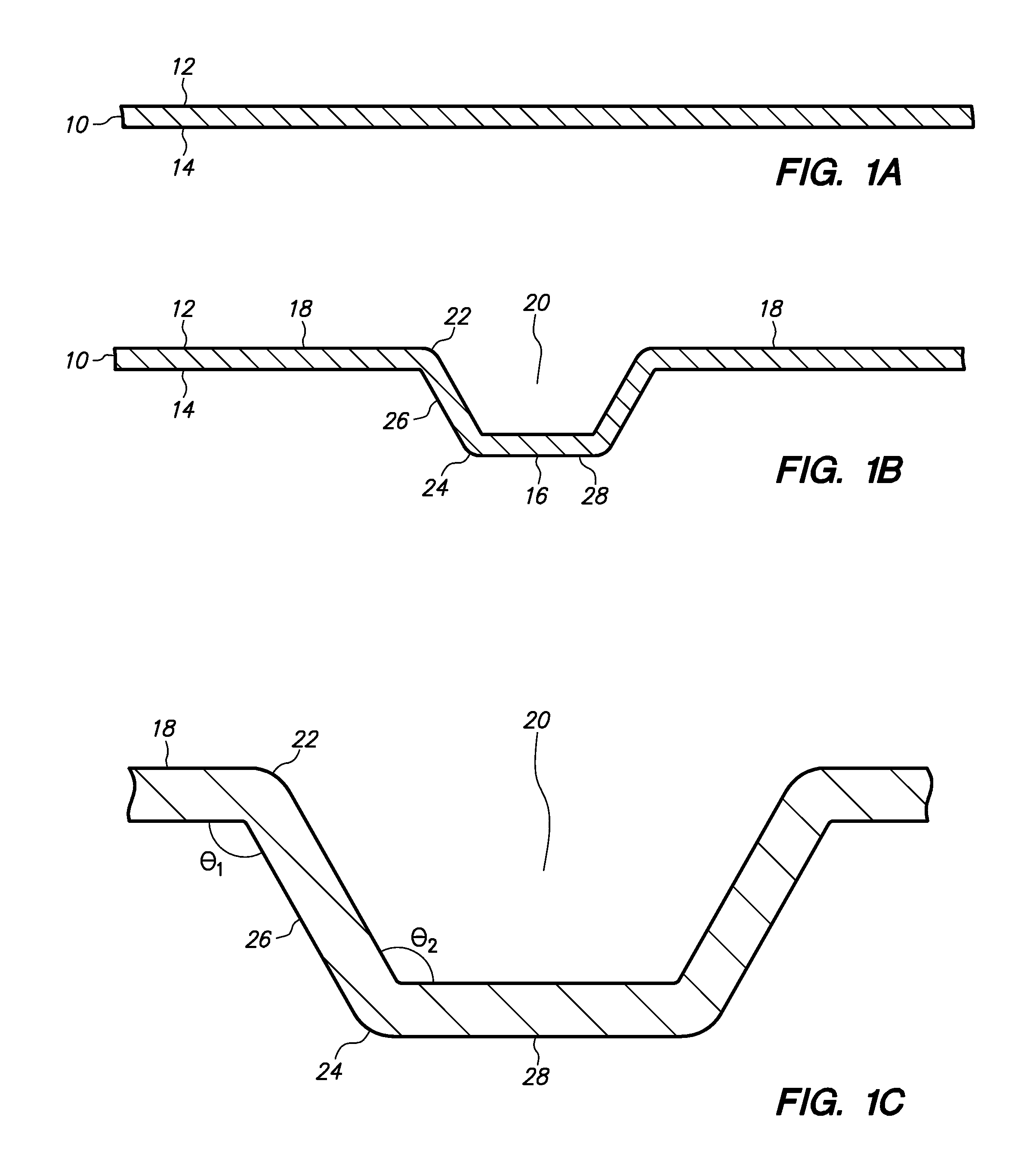
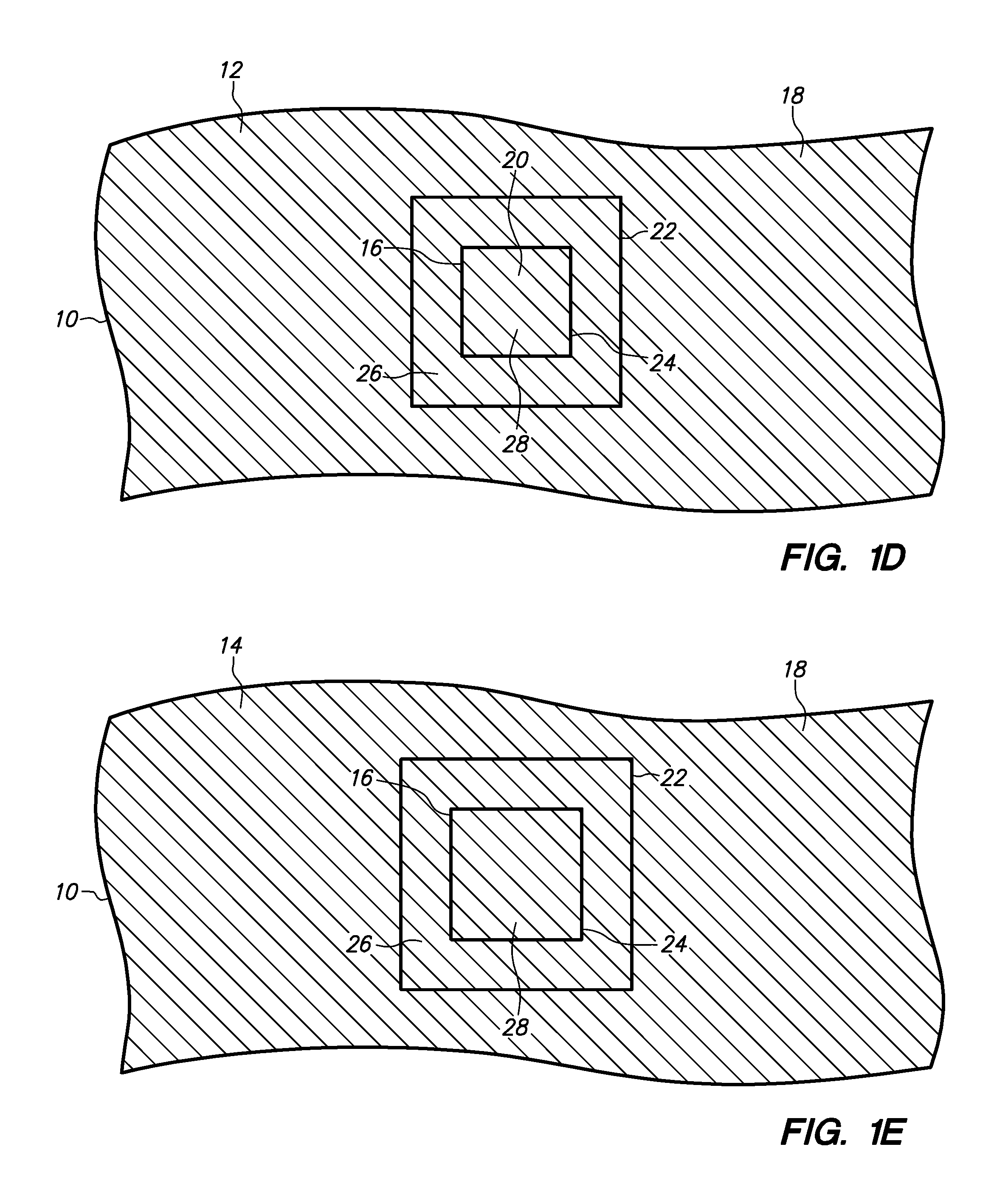
[0104]FIGS. 1A and 1B are cross-sectional views showing a method of making a bump and a ledge in accordance with an embodiment of the present invention, FIG. 1C is an enlarged cross-sectional view corresponding to FIG. 1B and FIGS. 1D and 1E are top and bottom views, respectively, corresponding to FIG. 1B.

[0105]FIG. 1A is a cross-sectional view of metal plate 10 which includes opposing major surfaces 12 and 14. Metal plate 10 is illustrated as a copper plate with a thickness of 150 microns. Copper has high thermal conductivity, good bondability and low cost. Metal plate 10 can be various metals such as copper, aluminum, alloy 42, iron, nickel, silver, gold, combinations thereof, and alloys thereof.

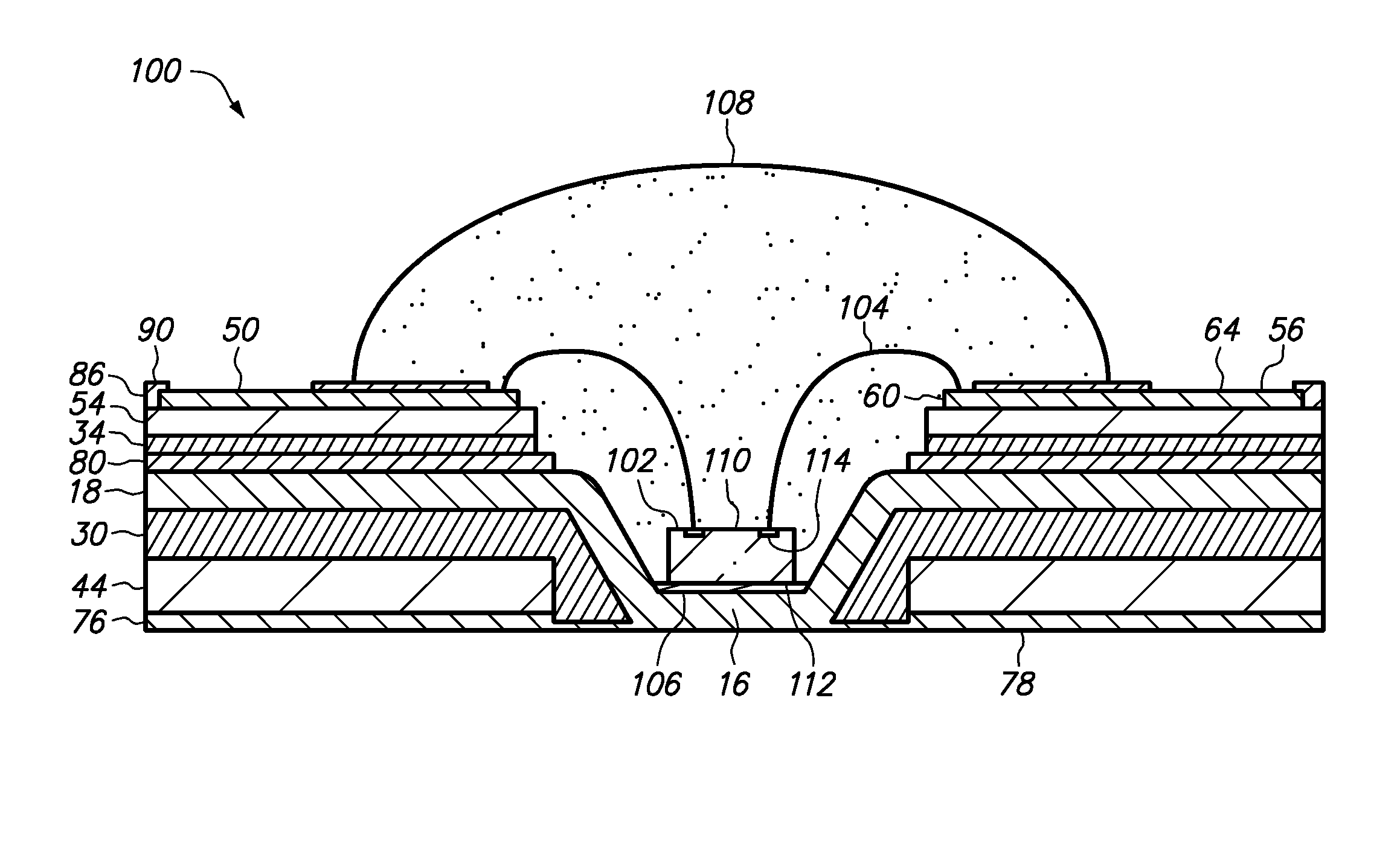
[0106]FIGS. 1B, 1C, 1D and 1E are cross-sectional, enlarged cross-sectional, top and bottom views, respectively, of metal plate 10 with bump 16, ledge 18 and cavity 20. Bump 16 and cavity 20 are formed by mechanically stamping metal plate 10. Thus, bump 16 is a stamped portion of metal pla...


PUM


Abstract

A method of making a semiconductor chip assembly includes providing a bump and a ledge, mounting a first adhesive on the ledge including inserting the bump into an opening in the first adhesive, mounting a conductive layer on the first adhesive including aligning the bump with an aperture in the conductive layer, then flowing the first adhesive between the bump and the conductive layer, solidifying the first adhesive, then providing a heat spreader that includes the bump, a base and the ledge, then mounting a second adhesive on the ledge, mounting a conductive trace that includes a pad and a terminal on the second adhesive, then mounting a semiconductor device on the bump in a cavity in the bump, electrically connecting the semiconductor device to the conductive trace and thermally connecting the semiconductor device to the heat spreader.

Description

CROSS-REFERENCE TO RELATED APPLICATIONS[0001]This application is a divisional of U.S. application Ser. No. 13 / 337,054 filed Dec. 24, 2011, which is a continuation-in-part of U.S. application Ser. No. 12 / 911,729 filed Oct. 26, 2010, which is incorporated by reference. U.S. application Ser. No. 13 / 337,054, 2011 application also claims the benefit of U.S. Provisional Application Ser. No. 61 / 531,013 filed Sep. 5, 2011, which is incorporated by reference.[0002]U.S. application Ser. No. 12 / 911,729 filed Oct. 26, 2010 is a continuation-in-part of U.S. application Ser. No. 12 / 616,773 filed Nov. 11, 2009 now U.S. Pat. No. 8,067,784 and a continuation-in-part of U.S. application Ser. No. 12 / 616,775 filed Nov. 11, 2009, each of which is incorporated by reference. U.S. application Ser. No. 12 / 911,729 filed Oct. 26, 2010 also claims the benefit of U.S. Provisional Application Ser. No. 61 / 350,036 filed Jun. 1, 2010 and U.S. Provisional Application Ser. No. 61 / 330,318 filed May 1, 2010, each of wh...

Claims


Application Information

Patent Timeline
Patent Type & Authority Patents(United States)
IPC IPC(8): H01L21/00
CPCH05K1/021H01L21/486H01L23/3677H01L2924/3025H01L2924/12041H01L2224/48091H01L2924/01028H01L2924/01014H01L2924/01013H01L2224/48227H01L2224/32245H01L2224/73265H01L2924/01087H01L2924/01019H01L24/45H01L24/48H01L33/483H01L33/642H01L2224/45144H01L2224/48225H01L2924/15153H05K3/4084H05K2201/0352H05K2201/0355H05K2201/10106H05K2203/049H05K2203/063H01L2924/00014H01L2924/00012H01L2924/00H01L24/73H01L2224/2929H01L2224/29339H01L2224/8385H01L2224/85205H01L2224/8592H01L2924/181H01L2924/0665
Inventor LIN, CHARLES W. C.WANG, CHIA-CHUNG
Owner BRIDGE SEMICON
Why Eureka
Try Eureka