
Semiconductor device and method of manufacturing semiconductor device

a semiconductor device and semiconductor technology, applied in the direction of semiconductor devices, basic electric elements, electrical equipment, etc., can solve the problems of high cost of soi wafer compared to the conventional single crystal silicon wafer, self-heating effect, etc., to reduce the occupied area per unit wafer area, increase current, and improve current

Inactive Publication Date: 2013-02-19
PS4 LUXCO SARL
View PDF8 Cites 15 Cited by
  • Summary
  • Abstract
  • Description
  • Claims
  • Application Information

AI Technical Summary

Benefits of technology

The semiconductor device described in this patent has a structure called SGTJ, which allows for the formation of small electrodes and short channel lengths. This results in improved ON currents without changing the threshold value and reduces the amount of space taken up on a wafer. Additionally, this device can realize some of the benefits of using an SOI substrate without the associated high costs. These benefits include reduced parasitic capacitance, prevention of latch-up, reduced junction leakage, and suppression of short channel effect.

Problems solved by technology

However, the SOI wafer is expensive compared to the conventional single crystal silicon wafer.
The SOI wafer has a problem in that a self-heating effect occurs because thermal conductivities of the embedded oxide film and the silicon layer are largely different.
However, manufacture of this structure has a problem in that it is difficult to dope by a conventional ion implantation.
On the other hand, if the body region has a channel formed therein, electric currents can not be controlled using only the small gate region.
However, a planar-type transistor that is a conventional all-around gate transistor has complicated manufacturing processes.
Further, it becomes a problem that a threshold voltage changes because the diameter of silicon pillar becomes wide as a result.
Therefore, Fin FET has a disadvantage in an area efficiency in the case of combination with or substitution of a conventional planar-type transistor.
Moreover, when manufacturing a transistor with an ultrashort channel length, it is disadvantageous to form the ultrashort channel length because conventional ion-implantation processes are used.
Since the shape of the transistor becomes higher in a direction perpendicular to the substrate or becomes longer in a direction of the substrate, the Fin FET has an unbalanced shape in which an original feature of the Fin FET cannot be utilized.
For this reason, there is a problem in that it is difficult to manufacture itself.
For this reason, there is a problem in that an occupied area per unit wafer area of the transistor becomes large.

Method used


Image

  • Semiconductor device and method of manufacturing semiconductor device
  • Semiconductor device and method of manufacturing semiconductor device
  • Semiconductor device and method of manufacturing semiconductor device

Examples


embodiment

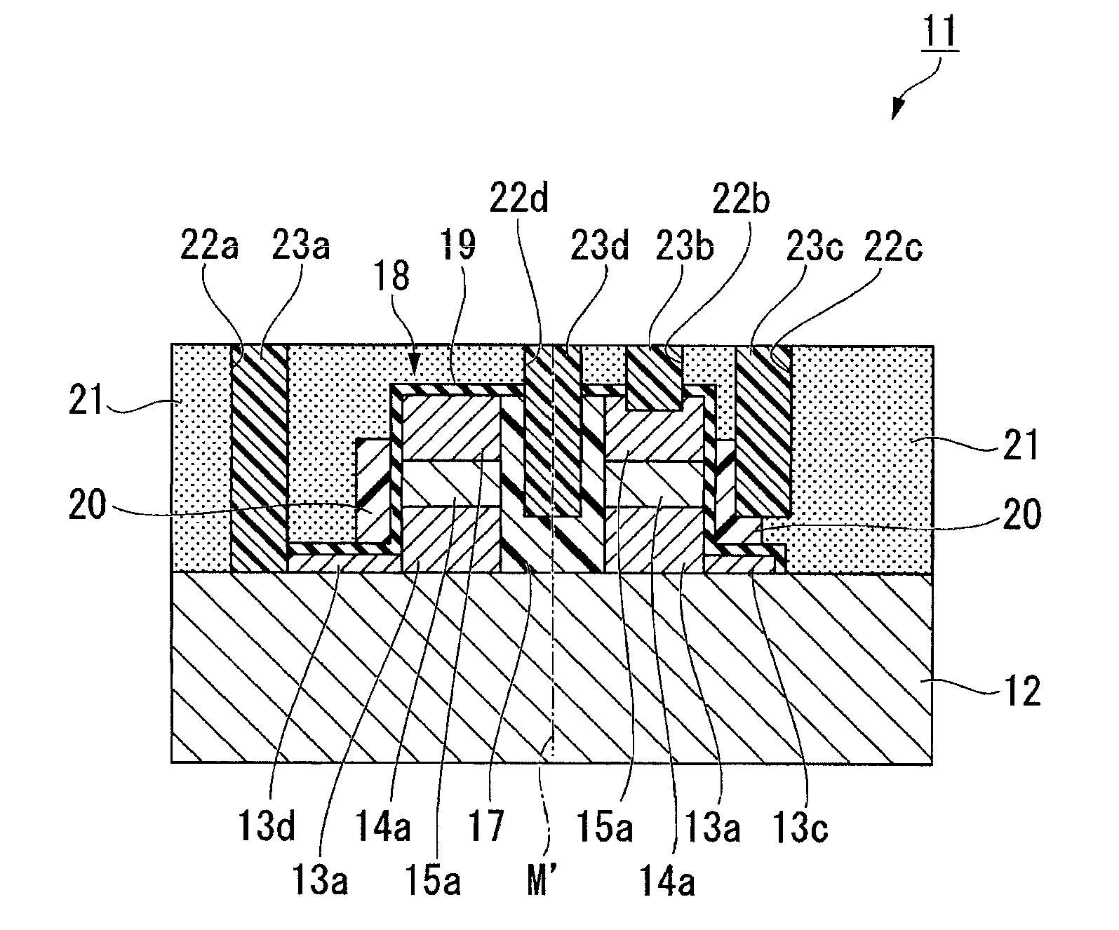
[0099]Next, it will be explained about an embodiment of the present invention in detail. The semiconductor device (STGJ) 11 having the structure shown in FIG. 3 was manufactured according to the processes shown in FIG. 4A to FIG. 7B.

[0100]FIG. 10 shows an electrical characteristic of the semiconductor device (STGJ) 11. The transistor has a gate length of 45 nm, a gate width of 220 nm, a thickness of the silicon layer of 20 nm, a gate insulating film of 5 nm, a carrier density of 3×1018 cm−3 of the body region forming the channel, a source and drain concentration of 2×1020 cm−3, the reverse bias gate electrode of 1×10 cm−3. A vertical axis is electric currents between a drain and a source, and a unit is a logarithmic expression expressed by ampere A. A horizontal axis is a voltage between a front gate and a source, and a unit is a linear expression expressed by voltage V. The voltage of the back gate is changed like −1.5V, −2.5V, 0V.

[0101]From a result shown in FIG. 10, it is found t...


PUM


Abstract

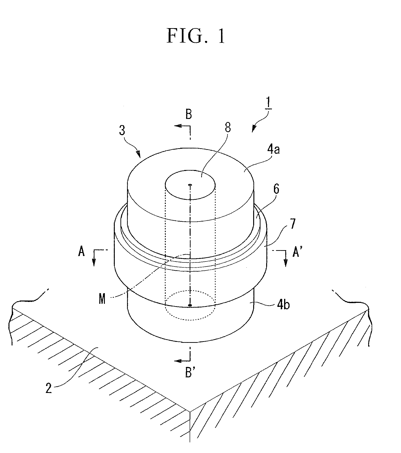
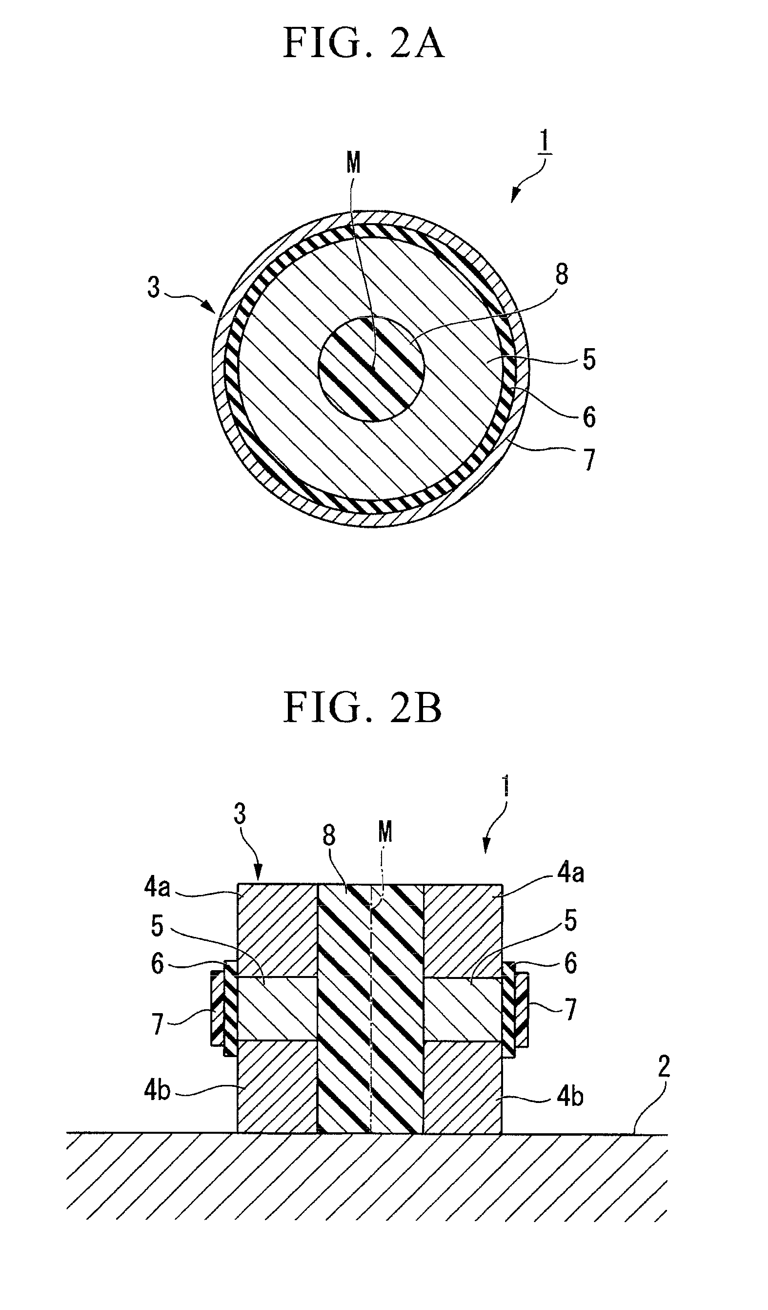
A semiconductor device includes a cylindrical main pillar that is formed on a substrate and of which a central axis is perpendicular to the surface of the substrate, source and drain diffused layers that are formed in a concentric shape centered on the central axis at upper and lower portions of the main pillar and made from a first-conduction-type material, a body layer that is formed at an intermediate portion of the main pillar sandwiched between the source and drain diffused layers and made from the first-conduction-type material, and a front gate electrode that is formed on a lateral face of the main pillar while placing a gate insulating film therebetween. Moreover, a back gate electrode made from a second-conduction-type material is formed in a pillar shape penetrating from an upper portion to a lower portion on an inner side of the main pillar.

Description

BACKGROUND OF THE INVENTION[0001]1. Field of the Invention[0002]The present invention relates to a semiconductor device and a method of manufacturing the semiconductor device. More particularly, the present invention relates to a semiconductor device having a vertical surround gate transistor (SGT) structure and a method of manufacturing the semiconductor device.[0003]Priority is claimed on Japanese Patent Application No. 2007-200868, filed Aug. 1, 2007, the content of which is incorporated herein by reference.[0004]2. Description of Related Art[0005]In recent years, semiconductor technology has been applied over a wide range. High integration and low power consumption are strongly requested in integrated circuits from a general electronic equipment such as a dynamic random access memory (DRAM) and a central processing unit (CPU) to a special purpose for an automotive engine control and a universal satellite. In order to realize drastic high integration for semiconductor integrated ...

Claims


Application Information

Patent Timeline
Patent Type & Authority Patents(United States)
IPC IPC(8): H01L29/66
CPCH01L29/66666H01L29/7827
Inventor HIGASHINO, TOSHIYUKI
Owner PS4 LUXCO SARL
Learn More