Method and system for integrated MEMS and NEMS using deposited thin films having pre-determined stress states

a technology of deposited thin films and integrated mems, which is applied in the direction of vacuum evaporation coating, test/measurement of semiconductor/solid-state devices, coatings, etc., can solve the problems of difficult to predict or control stress state, present state-of-the-art is considerably more modest, and advanced development programs seldom attempt to integrate mems with microelectronics. , to achieve the effect of enhancing the design potential of micro- and nano-dev

Active Publication Date: 2015-06-09
FOR NAT RES INITIATIVES
View PDF6 Cites 6 Cited by
  • Summary
  • Abstract
  • Description
  • Claims
  • Application Information

AI Technical Summary

Benefits of technology

[0016]The present invention allows tailorable, controlled, and reproducible stress states in thin films. The methods of the present invention can be applied to almost any known type and class of material that can be deposited by means of physical vapor deposition (PVD), which includes nearly all of the possible inorganic material choices for micro- and nano-device implementation. Specifically, the use of ion bombardment during deposition can achieve the goal of enabling control of the stress state of deposited films. Control over the deposition rate and pressure enable a further level of control over the resulting film stress-state to greatly enhance the design potential of micro- and nano-devices. Closed-loop control, whereby the stress of the film is able to be measured during deposition and the process parameters varied so as to obtain a pre-determined state of stress, is part of the present invention.
[0017]It is important to note that the present invention allows the temperature of the deposition to be constrained to some pre-determined level and the other process parameters adjusted accordingly to obtain a pre-determined and desired stress state in the deposited thin film. For example, many micro- and nano-fabrication process sequences require that the subst

Problems solved by technology

While this is the future trend of MEMS and NEMS technology, the present state-of-the-art is considerably more modest and usually involves a single discrete transducer element that is rarely integrated with microelectronics.
However, in both cases, the manufacturers of these MEMS technologies struggled to successfully integrate MEMS with microelectronics, resorted to using existing in-house microelectronics capabilities, and were pursuing relatively high volume MEMS markets.
Typically even the most advanced development programs seldom attempt to integrate the MEMS with microelectronics.
Moreover, using existing deposition techniques, the stress state has typically been difficult to either predict or control, especially in devices made from multilayer thin film structures.
Present understanding of the relationship between states of residual stress and the processing conditions through which thin films are deposited is typically very poor and at best highly qualitative.
Consequently, it is extremely difficult to design and fabricate devices if the mechanical properties of the materials used are not known, able to be controlled, and cannot be deposited reproducibly.
Furthermore, uncontrolled residual stresses can induce a variety of highly undesirable consequences, and include, but are not limited to, cracking, delamination, deformation, and microstructural changes in the materials.
The need to ensure thin film mechanical integrity through controlled stress states contin

Method used


Image

  • Method and system for integrated MEMS and NEMS using deposited thin films having pre-determined stress states
  • Method and system for integrated MEMS and NEMS using deposited thin films having pre-determined stress states
  • Method and system for integrated MEMS and NEMS using deposited thin films having pre-determined stress states

Examples


Embodiment Construction

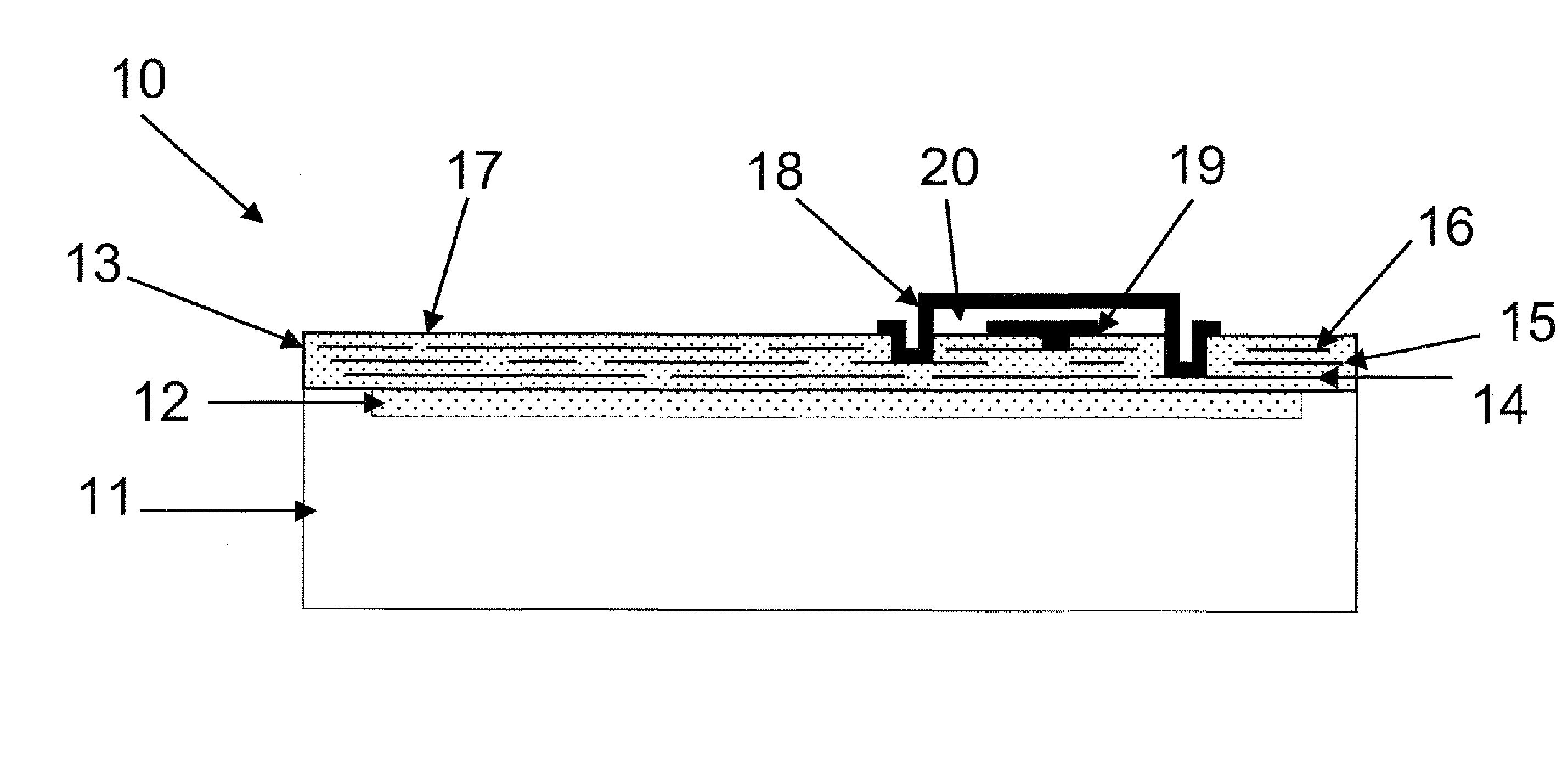
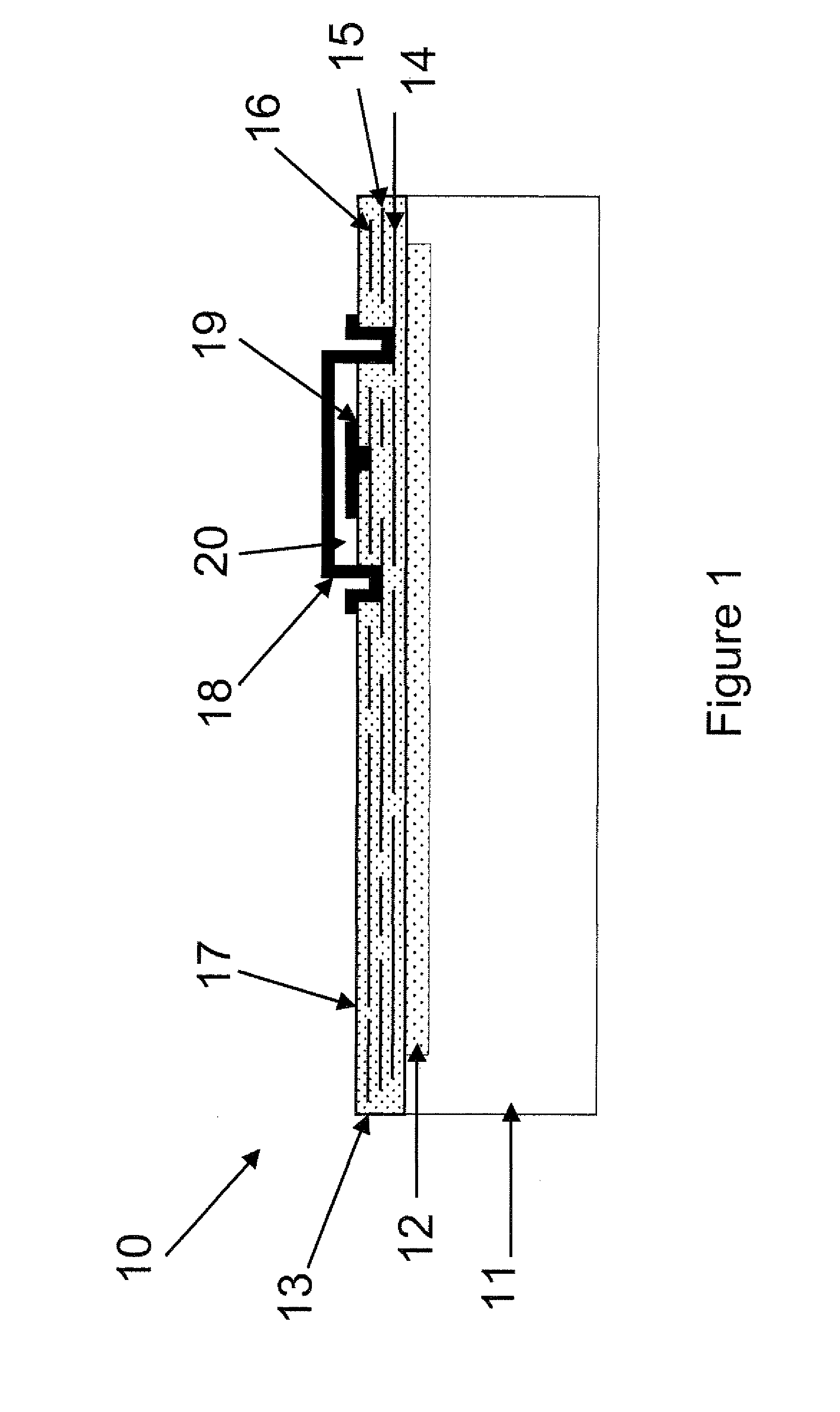
[0034]The major factors driving the integration of MEMS / NEMS with microelectronics are performance and cost. From the perspective of performance, merging electronics and MEMS / NEMS has some distinct advantages compared to having MEMS / NEMS and the electronics on separate die, that is the so-called “hybrid” approach. Integration greatly reduces parasitics, which are extremely important in capacitive-based sensors, such as accelerators, gyroscopes, microphones, etc. Also, the power consumption of integrated MEMS / NEMS devices is much lower compared to non-integrated, or hybrid schemes, which is particularly important for certain military applications, such as unattended ground sensors, handheld sensors, and many others.

[0035]Additionally, the noise level problems in integrated MEMS / NEMS are usually lessened. This is because small signals, such as present in capacitive-based MEMS / NEMS sensors, are more immune from background noise sources when the electronics are co-located with the MEMS / ...


PUM

PropertyMeasurementUnit
Temperatureaaaaaaaaaa

Abstract

A method and system are disclosed for controlling the state of stress in deposited thin films on microelectronics wafers for the integration of MEMS and NEMS devices with microelectronics. According to the method and system, various process parameters including: process pressure; substrate temperature; deposition rate; and ion-beam energies (controlled via the ion beam current, voltage, signal frequency and duty cycle) are varied using a step-by-step methodology to arrive at a pre-determined desired state of stress in thin films deposited using PVD at low temperatures and desired stress states onto wafers or substrates having microelectronics processing performed on them.

Description

CROSS-REFERENCES TO RELATED APPLICATIONS[0001]This application claims the benefit of Provisional Application No. 61 / 346,172, filed May 19, 2010.FIELD OF INVENTION[0002]The present invention is directed to a method and system for controlling the state of stress in deposited thin films on microelectronics wafers to a pre-determined value for the integration of MEMS and NEMS devices with microelectronics. This invention has application in microelectronics, nanoelectronics, micro-electro-mechanical systems (MEMS), nano-electro-mechanical systems (NEMS), photonics, and in other fields of endeavor that employ deposited thin films using physical vapor deposition (PVD) to implement integrated devices and structures.BACKGROUND OF THE INVENTION[0003]Advances in Micro-Electro-Mechanical Systems (MEMS) technology and Nano-Electro-Mechanical Systems (NEMS) technology promise to revolutionize commercial, defense, and industrial products by bringing together the computational capability of microel...

Claims


Application Information

Patent Timeline
IPC IPC(8): H01L21/00H01L21/02H01L21/66
CPCH01L22/12H01L21/02356H01L21/02274B81C1/00666B81B2207/015C23C14/22C23C14/3442C23C14/345C23C14/54H01L21/2855
Inventor HUFF, MICHAEL A.SUNAL, PAUL
Owner FOR NAT RES INITIATIVES
Why Eureka
Try Eureka