Microwave integrated circuit (MMIC) damascene electrical interconnect for microwave energy transmission

a technology of integrated circuits and electrical interconnections, which is applied in the direction of electrical apparatus, semiconductor devices, and semiconductor/solid-state device details. it can solve the problems of copper requiring a different patterning method, gold (au) based wiring schemes are not compatible with silicon foundries, and the total output power of mmics is very large, so as to achieve high power, prevent restructuring, and reduce the loss of microwave transmission lines

Active Publication Date: 2016-10-25
RAYTHEON CO
View PDF9 Cites 15 Cited by
  • Summary
  • Abstract
  • Description
  • Claims
  • Application Information

AI Technical Summary

Benefits of technology

[0011]The inventors have recognized that one of the reasons for using upper level metals for passive RF circuitry is they are typically the thickest metals formed during Damascene process, for example, 3 microns thick. With these thicker metals, RF or microwave transmission line loss can be lower in addition to handling high power when compared to the lower thinner metals. For example in RF power amplifier IC's the AC power output of several transistors will typically be combined to a single point before going off chip. This power combining is achieved by joining several microwave transmission lines. This thick metal interconnect layer or level (the microwave transmission lines) for level (or stage) M3 is typically 3 to 7 microns thick of un-interrupted copper bounded by the barrier layer used in the Damascene process on the bottom and top of metal for stage or level M3. One reason being that the thickest available un-interrupted bulk conductor of the metal interconnect layer will handle the most power will reduce the chances of high power microwave transmission line failure.
[0014]More particularly, the inventors have recognized that a single strip conductor can formed as multi-layer stack specifically designed with prevent electro-migration of the Cu metal wire under high power applications. In accordance with the disclosure, the inventors use a thin electrically conductive barrier layer (typically used for adhesion and to prevent Cu diffusion), and the thicker Cu layer (used for carrying current) and design a structure of stacked barriers and Cu layers such that the barrier layer also serves to prevent restructuring of the Cu (in addition to preventing Cu diffusion.
[0018]Thus, while the upper most metal interconnect for layer M3 of the MMIC of FIG. 1 is formed as a homogenous Damascene copper conducting interconnect layer, in accordance with one embodiment of the disclosure, this upper Damascene for stage or level M3 copper metal interconnect layer is formed as a stack of Damascene interconnect layers, each Damascene interconnect layer having a thin copper layer between a pair of barrier seed layers for the copper in the copper layer thus reducing the temperature fatigue of this Damascene metal interconnect metal for stage or level M3 of FIG. 1. Further, the inventors have recognized that the Damascene process may therefore be all the way from bottom via (Via-0) metal interconnect layer of the MMIC (FIG. 1) through to last Cu Metal interconnect stage or level (M3) and that the barrier seed layers can be used to control metal restructuring. Thus, the inventors have recognized that replacing the solid thick interconnect metal stage or level M3 of un-interrupted copper with a plurality of thinner stacks of barrier layers and copper layers (each one of the layers having a lower barrier metal layer) that the power handling power of the upper metal interconnect layer under extreme temperature cycling as when carrying microwave energy may be improved. Thus, the inventors have recognized that the Damascene process already used to form a single metal interconnect for each stage or level can be used as a sequence of a plurality of individual Damascene processes to form each metal interconnect as a stack of thinner metal layers itself thereby improving the power handling power of the upper metal interconnect layer under extreme temperature cycling as when carrying microwave energy.

Problems solved by technology

This combination of power density and periphery in turn leads to MMICs with very large total output power.
The high power density and total output power have posed reliability challenges (electrical and thermal) that have had to be solved at the material, device, on-chip interconnect, and module levels.
However, gold (Au) based wiring schemes are not compatible with silicon foundries due to both the high cost of Au and the fact that Au is essentially a contaminant in Si CMOS based processes.
However, copper requires a different method for patterning than aluminum because the lack of volatile copper compounds stifles plasma dry etching of Cu metal lines for interconnects.
A barrier metal layer must completely surround all copper interconnections, since diffusion of copper into surrounding materials would degrade their properties.
Since most of the RF energy propagates closer to the surface this is where the greatest temperature excursions and cycling of the bulk copper will occur and be a source of microwave transmission line failure.

Method used


Image

  • Microwave integrated circuit (MMIC) damascene electrical interconnect for microwave energy transmission
  • Microwave integrated circuit (MMIC) damascene electrical interconnect for microwave energy transmission
  • Microwave integrated circuit (MMIC) damascene electrical interconnect for microwave energy transmission

Examples


Embodiment Construction

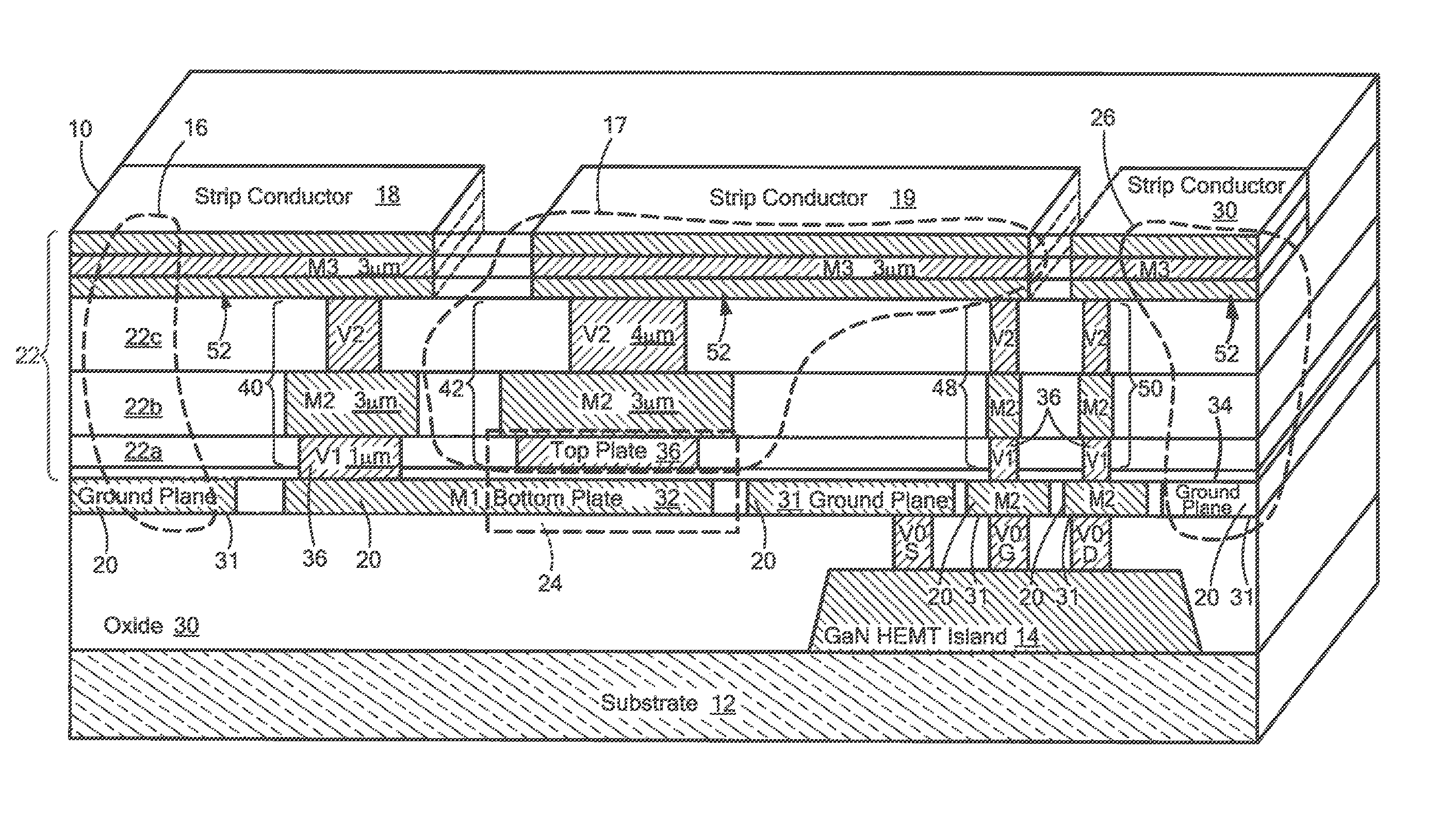
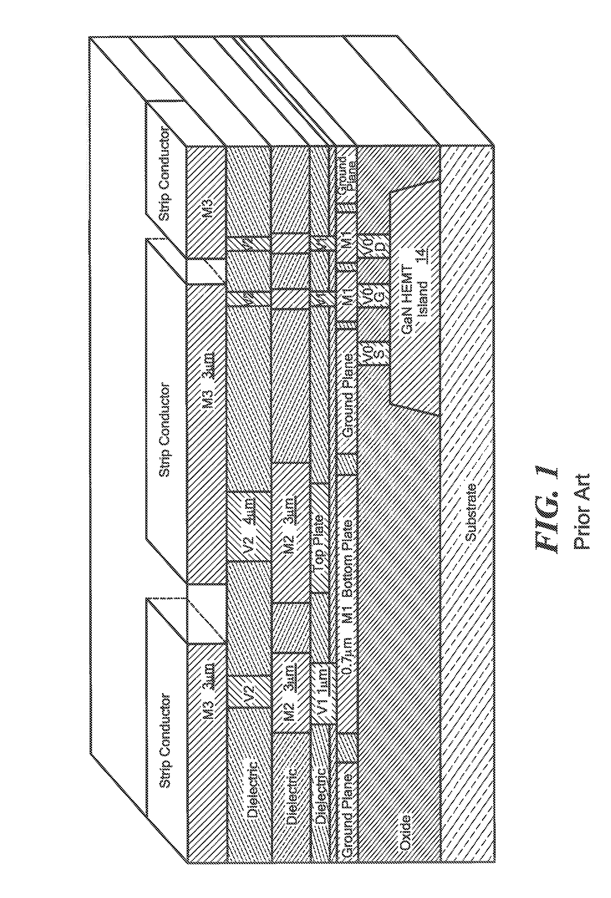
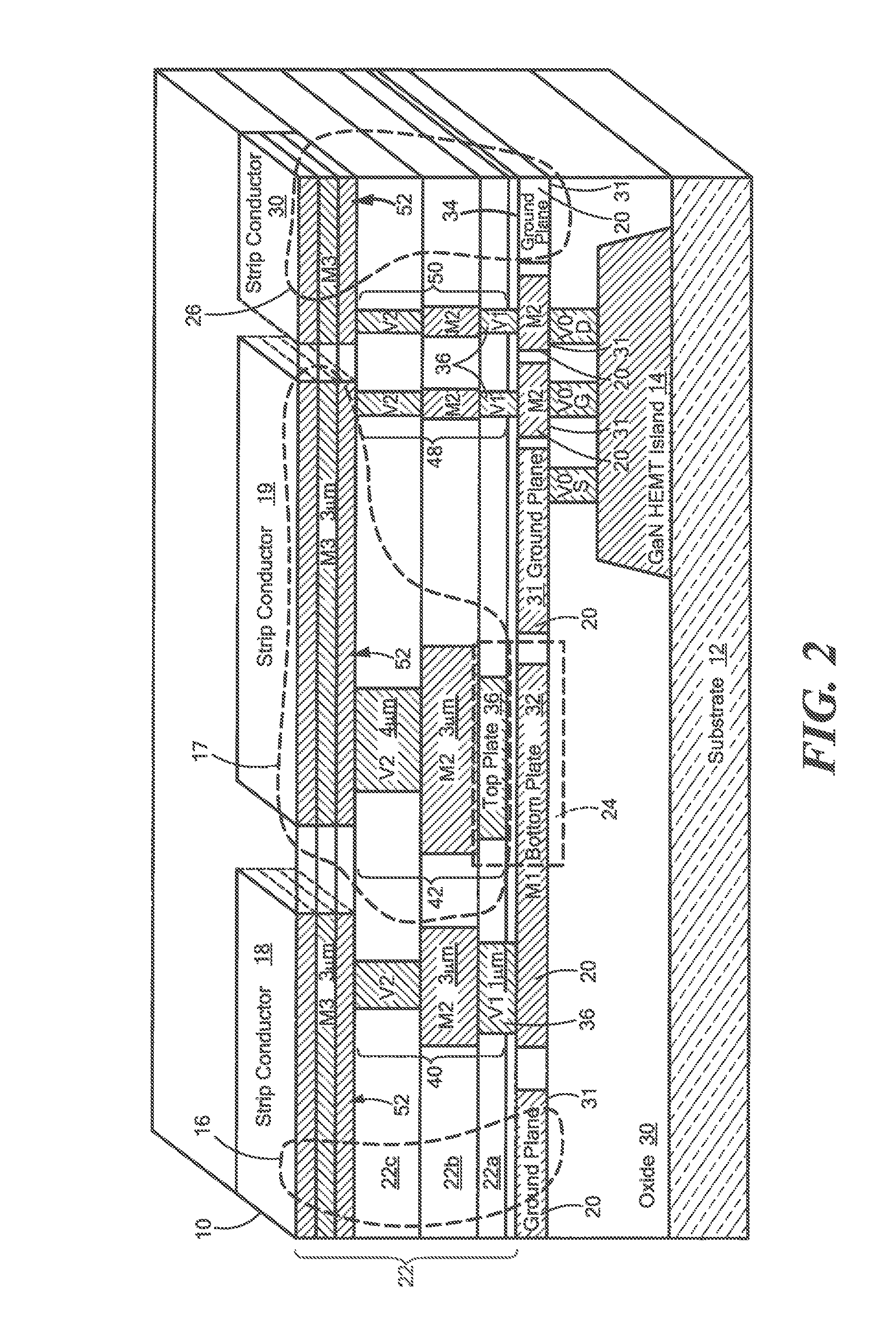
[0033]Referring now to FIG. 2, a MMIC chip 10 is shown having a substrate 12, here for example silicon, and a Field Effect Transistor (FET) 14, here a GaN FET, formed on the surface on the substrate 12. Here, for example, microwave energy is fed through an input microwave transmission line 16, here a strip transmission line having a strip conductor 18 separated from a ground plane conductor 20 by a dielectric structure 22 (to be described), to the gate electrode (G) of an amplifier GaN FET through a capacitor 24, here for example, a Metal Insulator Metal (MIM) capacitor and a microwave transmission line 17, here a strip transmission line having a strip conductor 19 separated from a ground plane conductor 20 by a dielectric structure 22; the FET 14 having a grounded source electrode (S); the drain electrode (D) being coupled to an output microwave transmission 26, here a strip transmission line having a strip conductor 30 separated from the ground plane conductor 20 by the dielectric...


PUM


Abstract

A semiconductor structure having a semiconductor layer having an active device therein. A dielectric structure is disposed over the semiconductor layer, such dielectric structure having open ended trench therein. An electrical interconnect level is disposed in the trench and electrically connected to the active device. A plurality of stacked metal layers is disposed in the trench. The stacked metal layers have disposed on bottom and sidewalls thereof conductive barrier metal layers.

Description

TECHNICAL FIELD[0001]This disclosure relates generally to monolithic microwave integrated circuits and more particularly to high power microwave transmission lines structures used in such circuits.BACKGROUND AND SUMMARY[0002]Over the last decade gallium nitride (GaN) high electron mobility transistors (HEMTs) have developed rapidly for use in power electronics and high power, high frequency (generally referred to as Radio Frequency (RF)) applications. In high power, high frequency applications, Monolithic Microwave Integrated Circuit (MMICs) have demonstrated power amplifiers (PAs) and low noise amplifiers (LNAs) with excellent characteristics at frequencies ranging from S-band to W-band and beyond. In general, the GaN PAs exhibit gain and efficiencies equivalent to GaAs PAs at ≧5 times the power density and often with very large output peripheries. This combination of power density and periphery in turn leads to MMICs with very large total output power.[0003]The high power density ...

Claims


Application Information

Patent Timeline
Patent Type & Authority Patents(United States)
IPC IPC(8): H01L23/66H01L23/528H01L23/532
CPCH01L23/66H01L23/528H01L23/53238H01L23/5329H01L2223/6683H01L2223/6627H01L21/76838H01L21/76847H01L23/5226H01L23/53295
Inventor LAROCHE, JEFFREY R.BETTENCOURT, JOHN P.KAZIOR, THOMAS E.IP, KELLY P.
Owner RAYTHEON CO
Why Eureka
Try Eureka