Erosion resistant pattern forming method, micro-pattern forming method using the same

A technology of resist patterns and fine patterns, which is applied in the direction of microlithography exposure equipment, instruments, electrical components, etc., can solve problems such as difficulty in resist patterns, difficulty in maintaining shapes with different thicknesses, and deterioration of heat resistance, etc. The number of engraving processes, excellent etching resistance, and good heat resistance

Inactive Publication Date: 2007-10-03
TOKYO OHKA KOGYO CO LTD
View PDF3 Cites 0 Cited by
  • Summary
  • Abstract
  • Description
  • Claims
  • Application Information

AI Technical Summary

Problems solved by technology

[0022] However, even if such a step-shaped resist pattern is formed using a resist material preferred in conventional liquid crystal display element production, it is difficult to achieve such a method because the etching resistance and heat resistance are not sufficient.
[0023] Specifically, as described above, because the step-shaped resist pattern is used as an etching mask before and after deformation, it is required to have high etching resistance, but forming such a resist pattern with high etching resistance Stepped resist patterns are more difficult
[0024] In addition, in order to make the resist pattern used in the manufacture of liquid crystal display elements withstand the etching process and injection process, post-baking treatment is sometimes performed to improve heat resistance, but the preferred resist in the conventional manufacture of liquid crystal display elements The reverse side of the material is cheap and highly sensitive, and the heat resistance tends to deteriorate, so the step-shaped resist pattern is flawed by the post-baking process, making it difficult to maintain the shape with different thicknesses

Method used


Image

  • Erosion resistant pattern forming method, micro-pattern forming method using the same
  • Erosion resistant pattern forming method, micro-pattern forming method using the same
  • Erosion resistant pattern forming method, micro-pattern forming method using the same

Examples


Embodiment 1

[0156] Prepare a positive photoresist composition.

[0157] Preparation (A) component: cresol novolac resin [obtained by condensation reaction of mixed phenols of m-cresol / p-cresol = 4 / 6 (molar ratio) and formaldehyde by a conventional method, weight average molecular weight (Mw) =5000 resin] 100 parts by mass, (B) component: [bis(2,3,5-trimethyl-4-hydroxyphenyl)-2-hydroxyphenylmethane] 10 parts by mass, (C) component: [Esterification reaction product of 1 mol of 2,3,4,4'-tetrahydroxybenzophenone and 2.34 mol of 1,2-naphthoquinonediazide-5-sulfonyl chloride] 29.7 parts by mass, (D) component: [PGMEA] 430 parts by mass, after uniformly dissolving the above-mentioned components (A) to (D), 400 ppm of BYK-310 (manufactured by Bikchemi Co., Ltd.) was blended therein as a surfactant, and the above-mentioned substances were filtered using a membrane filter with a pore size of 0.2 μm. A positive photoresist composition was prepared.

[0158] Using a resist coating apparatus [TR-360...

Embodiment 2

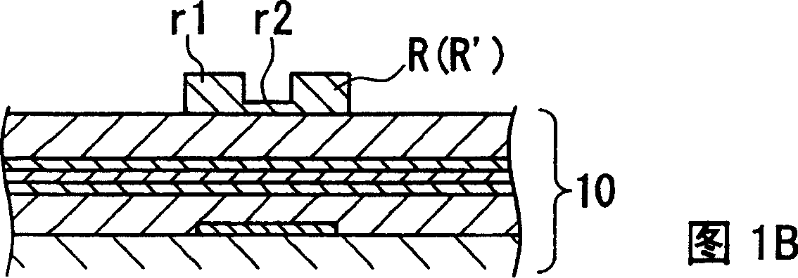
[0164] Using the same positive photoresist composition as in Example 1, the same steps as in Example 1 were used to form a step-shaped resist pattern. Wherein, the formation of the step-shaped resist pattern is made into a cross-sectional convex shape, and its size is that the thickness of the thick wall part is 2.0 μm, the thickness of the thin wall part is 0.8 μm, the entire width is 13 μm, and the width of the thin wall part is 5 μm.

[0165] The results of evaluating the heat resistance, dry etching resistance, and wet etching resistance of this step-shaped resist pattern are shown in Table 1 below.

Embodiment 3

[0167] After forming a step-shaped resist pattern in the same manner as in Example 1, a post-baking treatment was performed at 130° C. for 300 seconds on the other hand.

[0168] Table 1 below shows the results of evaluating the heat resistance, dry etching resistance, and wet etching resistance of the step-shaped resist pattern after the post-baking treatment.


PUM

PropertyMeasurementUnit
thicknessaaaaaaaaaa
thicknessaaaaaaaaaa

Abstract

The method for forming a resist pattern includes steps of: (A) forming a photoresist film on a substrate 10; (B) patterning the photoresist film into a pattern having a thick part r1 and a thin part r2 by way of photolithographic process including selective exposure; and (C) curing the resist with UV rays after patterning to form a step-like resist pattern R having the thick part r1 and the thin part r2.

Description

technical field [0001] The present invention relates to a method for forming a resist pattern, a method for forming a fine pattern using the method, and a method for manufacturing a liquid crystal display element. Background technique [0002] In the manufacture of a liquid crystal array substrate of a liquid crystal display element, a photolithography process using a photoresist film is used. [0003] 2 to 15 are diagrams showing examples of steps of manufacturing an α-Si (amorphous silicon dioxide) type TFT array substrate having the structure shown in FIG. 16 . In this example, first, a gate electrode layer 2' is formed on a glass substrate 1 as shown in Fig. 2 . [0004] Next, a photoresist film is formed on the gate electrode layer 2', and the photoresist film is patterned by a photolithography method. The photolithography method includes a process of selectively exposing through a mask, as shown in FIG. 3, a resist pattern R1 is formed (first photolithography process...

Claims


Application Information

Patent Timeline
Patent Type & Authority Patents(China)
IPC IPC(8): G03F7/20H01L21/00G02F1/133G03F7/40G02F1/136H01L21/306H01L21/3065H01L21/336H01L29/786
CPCG03F7/36H01L21/0274H01L27/1288
Inventor 森尾公隆
Owner TOKYO OHKA KOGYO CO LTD
Why Eureka
Try Eureka