Method of in-situ depositing high dielectric constant ferric oxide and metal film on indium phosphide material

A high dielectric constant, aluminum oxide technology, applied in the field of microelectronics, can solve the problems of thickness uniformity, poor repeatability of thickness between sheets, uneven thickness, and inability to achieve precise control, and achieve precise control of film thickness, Good quality and cost savings

Inactive Publication Date: 2007-11-14
XIDIAN UNIV
View PDF5 Cites 0 Cited by
  • Summary
  • Abstract
  • Description
  • Claims
  • Application Information

AI Technical Summary

Problems solved by technology

[0029] 1) This method cannot form mass production;
[0030] 2) Generated Al 2 o 3 Film thickness cannot be precisely controlled;
[0031] 3) The thickness uniformity of each part in the sheet and the thickness repeatability between sheets are poor;
[0032] 4) Al produced by anodic oxidation 2 o 3 The biggest problem is uneven thickness, that is, the aluminum side is rich in Al +3 Ionic membrane, and the oxygen-rich ion membrane is on the side of the electrolyte, and the insulating aluminum oxide layer is in the middle, so the thin film behaves as a PIN structure, which makes it have rectification characteristics, which is very unfavorable in application
[0061] The above two processes require many steps, so the work efficiency is low and the production cost is high. In addition to an EB evaporation table, a DC reactive sputtering table of hundreds of thousands to more than 1 million yuan is required, and dozens of At the same time, due to the existence of harmful gases in the etching, it not only causes harmful pollution to the environment, but also, the film is exposed to the atmosphere 8 times during the processing process, which affects the electrical characteristics of the device, especially the stability of the device. And reliability and pass rate will have a great impact; in addition, use DC reactive sputtering equipment to deposit Al 2 o 3 A large amount of very expensive high-purity gas, such as high-purity Ar, is required, and Al is deposited 2 o 3 The uniformity and repeatability are not very good, the deposition rate and film thickness cannot be directly monitored, and the purpose of precise control cannot be achieved

Method used


Image

  • Method of in-situ depositing high dielectric constant ferric oxide and metal film on indium phosphide material
  • Method of in-situ depositing high dielectric constant ferric oxide and metal film on indium phosphide material
  • Method of in-situ depositing high dielectric constant ferric oxide and metal film on indium phosphide material

Examples


Embodiment 1

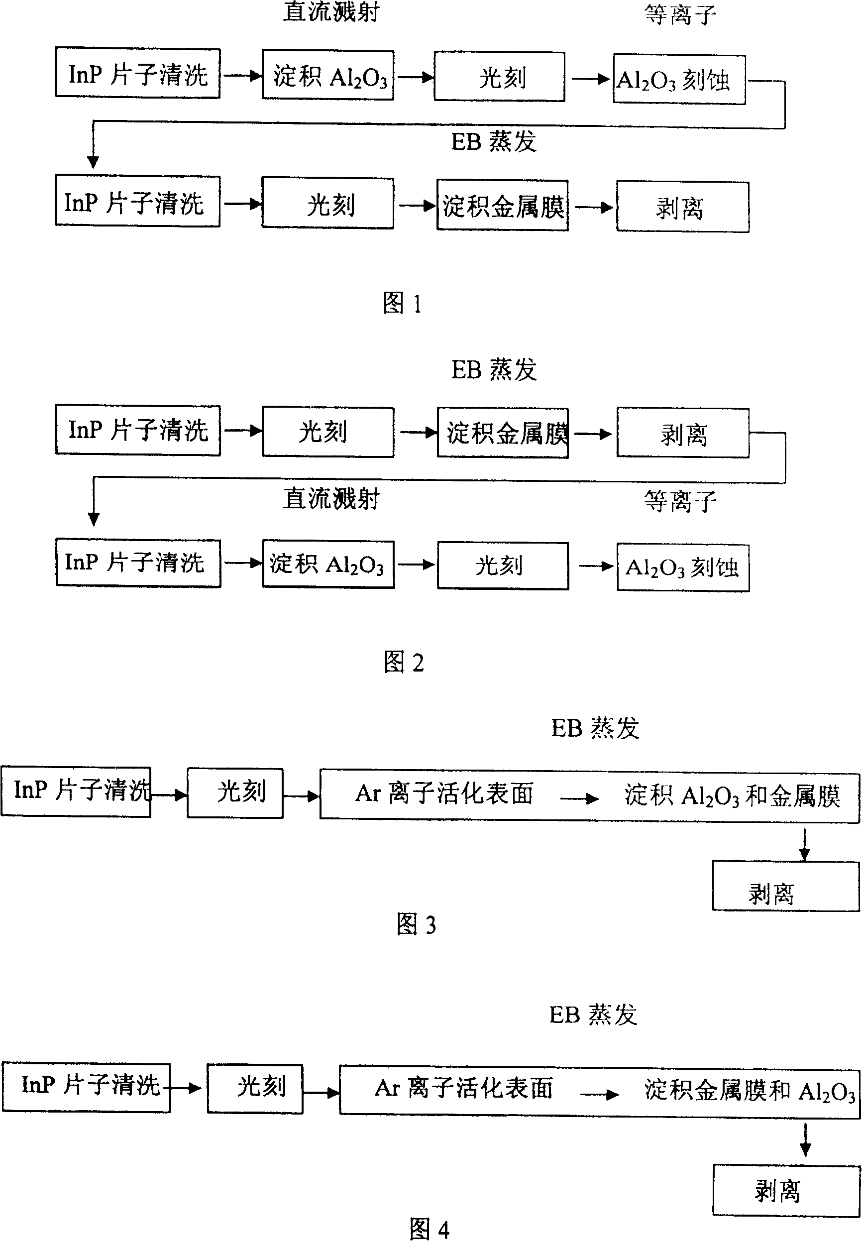
[0095] On InP wafers, evaporate Al first 2 o3 After evaporating the metal film, the metal film is deposited by two layers of Cr (chromium) and Au (gold) to form a composite metal film, that is, the Al 2 o 3 Evaporate, and then carry out Cr / Au in-situ evaporation, the specific process is:

[0096] In the first step, the substrate of the InP-based material is cleaned and dried at T=120°C for 5 minutes;

[0097] The second step is to photolithographically pattern the cleaned InP substrate;

[0098] In the third step, put the photoetched film into the reaction chamber of the electron beam evaporation table, and vacuumize it to 1.8×10 -3 Above Pa, and use argon ions to activate the surface of the InP substrate for 20 seconds to enhance the adhesion between the steamed object and the sheet, and then carry out Al in accordance with the following process conditions 2 o 3 The evaporation of the film, and then the evaporation of Cr and Au metal films in sequence:

[0099] (1)Al 2...

Embodiment 2

[0123] On InP-based materials, evaporate Al first 2 o 3 , after evaporating Al (aluminum) metal, the specific process is:

[0124] The first step is to clean the substrate of the InP-based material and dry it at T=120°C for 5 minutes; the second step is to photolithographically pattern the cleaned InP substrate;

[0125] In the third step, put the photoetched film into the reaction chamber of the electron beam evaporation table, and vacuumize it to 1.8×10 -3 Above Pa, and use argon ions to activate the surface of the InP substrate for 20 seconds to enhance the adhesion between the steamed object and the sheet, and then carry out Al in accordance with the following process conditions 2 o 3 The evaporation of the film, and then the evaporation of the Al metal film:

[0126] (1)Al 2 o 3 Membrane evaporation conditions

[0127] a, will be equipped with Al 2 o 3 The crucible of the material is placed in the heating position, and the electron gun is placed at a high voltage...

Embodiment 3

[0142] On the InP substrate, the Ge (germanium) / Au (gold) / Ni (nickel) / Au (gold) composite metal film is evaporated in sequence, and then the Al 2 o 3 The in-situ evaporation of the film, the specific process is:

[0143] In the first step, the substrate of the InP-based material is cleaned and dried at T=120°C for 5 minutes;

[0144] The second step is to photolithographically pattern the cleaned InP substrate;

[0145] In the third step, put the photoetched film into the reaction chamber of the electron beam evaporation table, and vacuumize it to 1.8×10 -3 Above Pa, and use argon ions to activate the surface of the InP substrate for 20 seconds to enhance the adhesion between the steamed object and the sheet, and then perform Ge / Au / Ni / Au / Al in sequence according to the following process conditions 2 o 3 Evaporation of the film;

[0146] (1) Conditions for evaporating Ge metal film

[0147] a. The vacuum degree of the reaction chamber is maintained at 1.8×10 -3 Above Pa,...


PUM


Abstract

This invention discloses a method for depositing high dielectric constant Al2O3 and a metallic film in-situ on an InP material, which applies EB vacuum evaporation, takes pure Al2O3 particles of over 99.99% and a metal as the evaporation materials including: cleaning the chip first, carrying out photoetching and evaporating a window then putting the chip in a mask of the EB evaporation stand to be vacuum-pumped to over 1.8x10⁻³Pa, activating the surface of the InP chip with Ar ions, then setting the density and coefficient of them, setting the voltage for evaporation at 10kv and adding different currents based on the materials to carry out the evaporation and deposition of the film and the metal film to reduce the current to zero after the thickness of the films reaches to a pre-designed value to leave necessary part of the AL2O3 and the metal.

Description

technical field [0001] The invention belongs to the technical field of microelectronics, and relates to the process treatment in the manufacture of compound material devices, in particular to an in-situ deposition of aluminum oxide with high dielectric constant (high κ) on an indium phosphide (InP) base (Al 2 o 3 ) and metal film methods. Background technique [0002] With the requirement for high speed, the size of MOSFET is shrinking continuously, which leads to a corresponding reduction in the thickness of the gate oxide layer. However, when the thickness of the gate oxide layer is less than 20 Ȧ, a significant quantum tunneling effect will be caused, resulting in a gate leakage current that affects device performance. In the case of the same equivalent thickness of the gate dielectric, if a high κ material is used instead of SiO 2 As a gate dielectric, it can significantly reduce the gate leakage current caused by direct tunneling. [0003] Among many high κ materia...

Claims


Application Information

Patent Timeline
Patent Type & Authority Patents(China)
IPC IPC(8): H01L21/283H01L21/768H01L21/316H01L21/3205C23C14/30
Inventor 郝跃谢永桂冯倩王冲龚欣李亚琴
Owner XIDIAN UNIV
Why Eureka
Try Eureka