
A diamond film flat field emission cathode and method for making same
A technology of diamond film and emitting cathode, which is applied in cold cathode manufacturing, electrode system manufacturing, discharge tube/lamp manufacturing, etc., can solve problems such as low emission threshold and current density, large influence of ambient temperature, and unstable emission performance. Achieve the effects of simple preparation method, reduced recombination, and stable and consistent emission characteristics
Patent Information
- Authority / Receiving Office
- CN · China
- Patent Type
- Patents(China)
- Current Assignee / Owner
- Publication Date
- 2008-05-28
- Estimated Expiration
- Not applicable · inactive patent
Smart Images
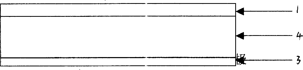
Figure 1 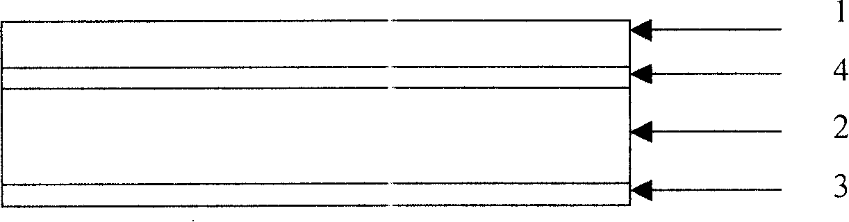
Figure 2
Abstract
Description
technical field
[0001] The invention belongs to a field emission cathode, in particular to a metal silicide (such as CoSi 2 、TiSi 2 、FeSi 2 、TaSi 2 、MoSi 2 、WSi 2 、NiSi 2 etc.) a transition layer and a diamond thin film, a planar field emission cathode used in the field of flat panel display and a manufacturing method thereof. Background technique
[0002] The diamond film planar field emission cathode made in the prior art is made of doped or non-doped diamond film material, with metal or single crystal silicon as the substrate, a layer of diamond film is grown on it, and the measurement is set on the other side of the substrate. The electrode uses the excellent physical and chemical properties of the diamond film, such as wide bandgap and electronegativity, to make a field emission cathode, and realizes electron emission on the surface of the diamond film under the action of an external electric field. Among them, the diamond film planar cathode made on silicon is g...
Examples
Embodiment 1
[0034]The specific structure of the diamond film planar field emission cathode of this embodiment can be found in figure 2 A polished N-type (001) single crystal silicon wafer is used as the substrate 2, and a layer of 50nm-thick metal silicide CoSi is grown on one side of the substrate 2 by the molecular beam epitaxy method. 2 4. The growth conditions are: use gas containing Si and Co as the source, and the gas pressure is 5×10 -9 Torr, the substrate temperature is 500 degrees, and the growth time is 8 minutes. at CoSi 2 A diamond film 1 with a thickness of 0.5 μm is grown on the surface by a microwave plasma chemical vapor deposition method, and the growth conditions are as follows: first, the diamond is nucleated, a negative bias voltage is applied to -140V, and the mixing ratio of methane / hydrogen is 10:100 by volume; The substrate temperature is 700°C, the reaction pressure is 30mbar, the microwave power is 1000W, and the nucleation time is 17 minutes; secondly, the d...
Embodiment 2
[0036] The specific structure of the planar diamond film field emission cathode of this embodiment can be found in figure 2 , the substrate 2 is made of polished metal Mo, and a layer of metal silicide TiSi with a thickness of 80 nm is grown on one side of the substrate 2 by reactive sputtering method. 2 4. The growth conditions are: the substrate temperature is 850 degrees, the silicon target sputtering power is 200W, the Ti target sputtering power is 80W, the flow rate of Ar is 20sccm, and the pressure is 1×10 -2 Torr, the sputtering time is 10 minutes, the sample is taken out after sputtering, in 1:1 H 2 SO 4 and H 2 o 2 Medium corrosion for 30 minutes can obtain high-purity C54 phase TiSi 2 membrane. At TiSi 2 A diamond film 1 with a thickness of 1 μm is grown on the surface by hot filament chemical vapor deposition method. The growth conditions are as follows: first, the diamond is nucleated, the temperature of the filament is 2000 degrees, the negative bias volta...
Embodiment 3
[0038] The specific structure of the planar diamond film field emission cathode of this embodiment can be found in figure 2 A polished N-type (001) single crystal silicon wafer is used as the substrate 2, and a layer of metal silicide FeSi with a thickness of 60 nm is grown on one side of the substrate 2 by ion implantation and annealing method. 2 4. Growth conditions: substrate temperature is 350 degrees, Fe + The injection energy is 200KV, and the metering is 2×10 17 / cm 2 , 1000 degrees annealing time 20 seconds after taking out the sample, in 1:1 H 2 SO 4 and H 2 o 2 Medium corrosion for 30 minutes, high purity FeSi can be obtained 2 membrane. In FeSi 2 A diamond film 1 with a thickness of 1 μm was grown on the surface by a hot filament chemical vapor deposition method, and the growth conditions were the same as those in Example 2. On the other side of the substrate 2, an Au / Ni electrode 3 was deposited by vacuum evaporation. The thickness of Ni was 50nm, and the...