

Process for preparing silumin electronic package materials
An electronic packaging material, high-silicon aluminum alloy technology, applied in the direction of circuits, electrical components, electrical solid devices, etc., can solve problems such as increased heating rate, increased circuit operating temperature, and increased component failure rate, and achieves a state of interface bonding Effects of improving, increasing thermal conductivity, and improving characteristics
- Summary
- Abstract
- Description
- Claims
- Application Information
AI Technical Summary
Problems solved by technology
Method used
Image

Examples
Embodiment 1
[0019] A) Powder preparation
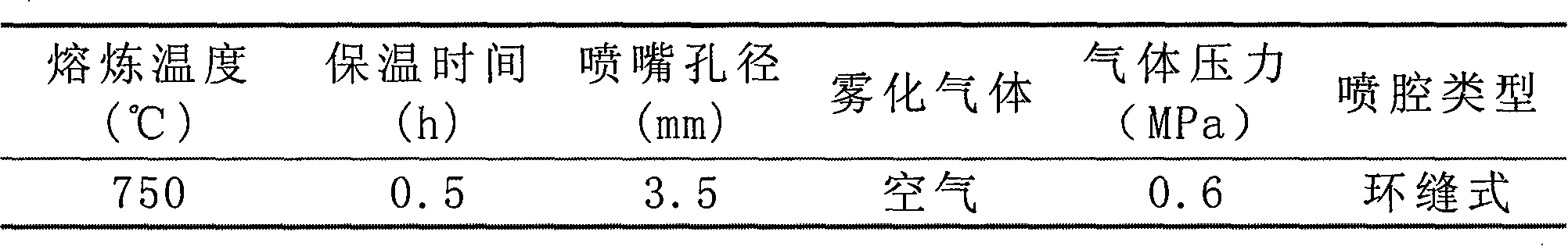
[0020] Industrial pure aluminum and high-purity silicon are melted in an induction furnace with a mass ratio of 8.8:1.2, heated to 750°C, fully stirred, and covered with a flux (30% NaCl + 47% KCl + 23% cryolite by mass percentage). Slag, and with hexachloroethane (C 2 Cl 6 ) outgassing. The metal droplets are injected into the spray device through the leak nozzle, and the metal droplets atomized by high-pressure nitrogen gas are directly sprayed into the high-pressure water flow 200mm away from the nozzle. After cooling, the water flow containing Al-Si alloy powder passes through the screen and leaks out. Miscellaneous materials flow into a high-speed rotary dryer for dehydration treatment, and the required Al-12Si alloy powder is obtained after drying and sieving. The powder-making process parameters are attached in Table 1.
[0021] Table 1 Milling Process Parameters
[0022]
[0023] B) Ball milling process of powder
[0024] Put the ...
Embodiment 2
[0030] A) Powder preparation
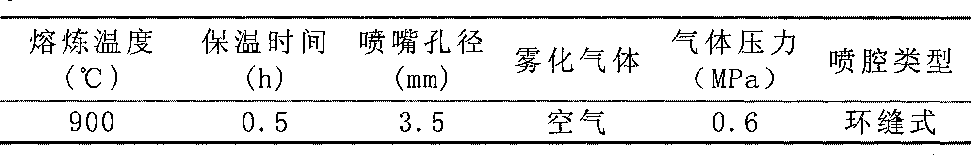
[0031] Industrial pure aluminum and high-purity silicon are melted in an induction furnace according to a mass ratio of 8:2, heated to 900°C, fully stirred, and covered with a flux (30% NaCl+47%KCl+23% cryolite by mass percentage) Slag, and with hexachloroethane (C 2 Cl 6 ) outgassing. The metal droplets are injected into the spray device through the leak nozzle, and the metal droplets atomized by high-pressure nitrogen gas are directly sprayed into the high-pressure water flow 200mm away from the nozzle. After cooling, the water flow containing Al-Si alloy powder passes through the screen and leaks out. Miscellaneous flows into the high-speed rotary dryer for dehydration treatment, and the required Al-20Si alloy powder is obtained after drying and sieving. The powder-making process parameters are attached in Table 2.
[0032] Table 2 Milling Process Parameters
[0033]
[0034] B) Ball milling process of powder
[0035] Put the prepared ...
Embodiment 3
[0041] A) Powder preparation
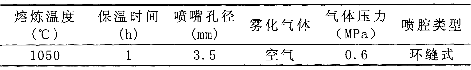
[0042]Industrial pure aluminum and high-purity silicon are melted in an induction furnace with a mass ratio of 7.4:2.6, heated to 1050°C, fully stirred, and covered with a flux (30% NaCl+47% KCl+23% cryolite by mass percentage) Slag, and with hexachloroethane (C 2 Cl 6 ) outgassing. The metal droplets are injected into the spray device through the leak nozzle, and the metal droplets atomized by high-pressure nitrogen gas are directly sprayed into the high-pressure water flow about 200mm away from the nozzle. After cooling, the water containing Al-Si alloy powder flows through the screen and leaks. The debris is flowed into a high-speed rotating drier for dehydration treatment, and the required Al-26Si alloy powder is obtained after drying and sieving. The powder-making process parameters are attached in Table 3.
[0043] Table 3 Milling Process Parameters
[0044]
[0045] B) Ball milling process of powder
[0046] The prepared Al-26Si al...
PUM
| Property | Measurement | Unit |
|---|---|---|
| density | aaaaa | aaaaa |
Abstract
Description
Claims
Application Information