Laminated filter based on MEMS technology

A filter and stacked technology, which is applied in the coupling of waveguide devices, resonators, and optical waveguides, can solve the problems of attenuation performance that cannot meet the requirements of use and large volume, and achieve shortened design cycles, small volume, and reduced costs. Effect

Active Publication Date: 2008-11-19
NO 55 INST CHINA ELECTRONIC SCI & TECHNOLOGYGROUP CO LTD
View PDF4 Cites 0 Cited by
  • Summary
  • Abstract
  • Description
  • Claims
  • Application Information

AI Technical Summary

Problems solved by technology

[0004] The purpose of the present invention is to design a filter that can work at the high end of the microwave frequency band, has a small overall structure, and has good out-of-band suppression performance, aiming at the problems of large volume and attenuation performance that cannot meet the requirements of use in the current filter based on traditional technology. A stacked filter based on MEMS technology with low insertion loss, high process precision, easy integration, and mass production

Method used


Image

  • Laminated filter based on MEMS technology
  • Laminated filter based on MEMS technology
  • Laminated filter based on MEMS technology

Examples


Embodiment

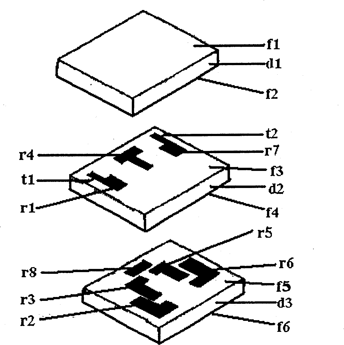
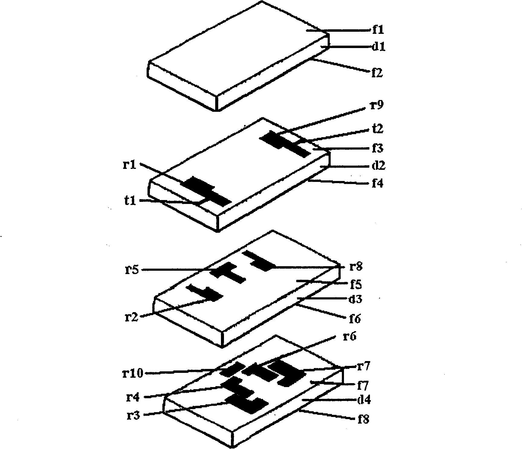
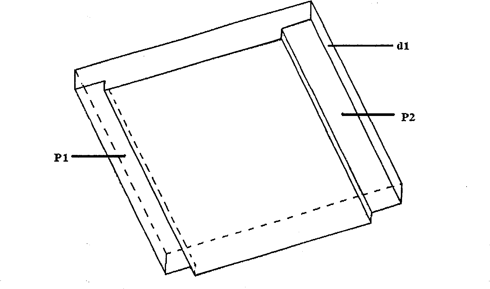
[0047] (1) The dielectric layer is a high-resistance silicon wafer, and a 3-layer stacked filter using a silicon-silicon bonding process:

[0048] A Φ4″525μm thick silicon wafer with a resistivity of 3000Ω·cm is thinned to 400μm thick by grinding and polished to ensure a certain degree of flatness and smoothness. Form t1 and r1 on one surface by photolithography and etching processes , r4, r7, t2 patterns of shallow grooves and steps p1, p2. Among them, the shallow grooves of t1, r1, r4, r7, t2 patterns are about 5 μm deep; the steps p1, p2 are about 100 μm deep, and use photolithography and etching Process forms scribing and alignment mark pattern on its other side. Utilize photolithography and metallization process to form r1, t1, r4, r7, The metal transmission line pattern of t2, and the alignment mark pattern is formed on the other side by photolithography and etching process. The surfaces of the above two silicon wafers without alignment marks are bonded together, and th...


PUM


Abstract

This invention discloses an overlay filter based on the MEMS technology in a distributed coupling line structure, in which, two earth surfaces are set above a first medium layer and under a third medium layer, interstage coupling resonators and input-output ends are placed in the middle of the medium layers, signals realize filtration performance by same layer plane coupling resonance and that between layers, the input and output ends are in a tap line structure, the middle coupling line is led to the cross coupling so as to strengthen the stopband attenuation performance, and thickness control of the medium layers, the patterns on the medium layers and alignment and assembly of the layers are formed by MEMS microprocess.

Description

technical field [0001] The invention relates to a stacked wave filter, especially a filter made of high-resistance silicon or glass material, specifically a stacked filter based on MEMS technology with good stop band attenuation and convenient manufacture . Background technique [0002] Microwave filter design requires small size, small insertion loss, high out-of-band rejection, and good impedance matching characteristics. At the same time, low cost and mass production are also required. The types of microwave filters mainly include lumped element (inductor, capacitor) form, distributed transmission line type, ceramic, cavity type, etc. In satellite, communication, aviation, aerospace and other systems, electronic systems are required to be small in size, high in reliability and low in cost. Today, with the use of large-scale integrated circuits, the integration of passive components such as microwave filters has become the bottleneck of the system. The common problem of...

Claims


Application Information

Patent Timeline
Patent Type & Authority Patents(China)
IPC IPC(8): H01P1/20H01P7/08H01P7/00B81B7/02
Inventor 朱健郁元卫张勇
Owner NO 55 INST CHINA ELECTRONIC SCI & TECHNOLOGYGROUP CO LTD
Why Eureka
Try Eureka