
Method for preparing micron/submicron metal ring and open-mouth metal ring

A metal ring and sub-micron technology, applied in chemical instruments and methods, separation methods, microstructure technology, etc., can solve the problems of complex micromachining technology, high cost, and long time consumption of equipment, and achieve low equipment requirements and low cost , good effect of monodispersity

Inactive Publication Date: 2009-06-03
NANJING UNIV
View PDF4 Cites 0 Cited by
  • Summary
  • Abstract
  • Description
  • Claims
  • Application Information

AI Technical Summary

Problems solved by technology

At present, the methods for preparing micron / submicron metal rings and split rings mainly include photolithography, electron beam or ion beam etching, focused ion beam direct writing, microcontact printing, etc. Most of them require complex micromachining technology, which is time-consuming and costly. high

Method used


Image

  • Method for preparing micron/submicron metal ring and open-mouth metal ring
  • Method for preparing micron/submicron metal ring and open-mouth metal ring
  • Method for preparing micron/submicron metal ring and open-mouth metal ring

Examples


Embodiment 1

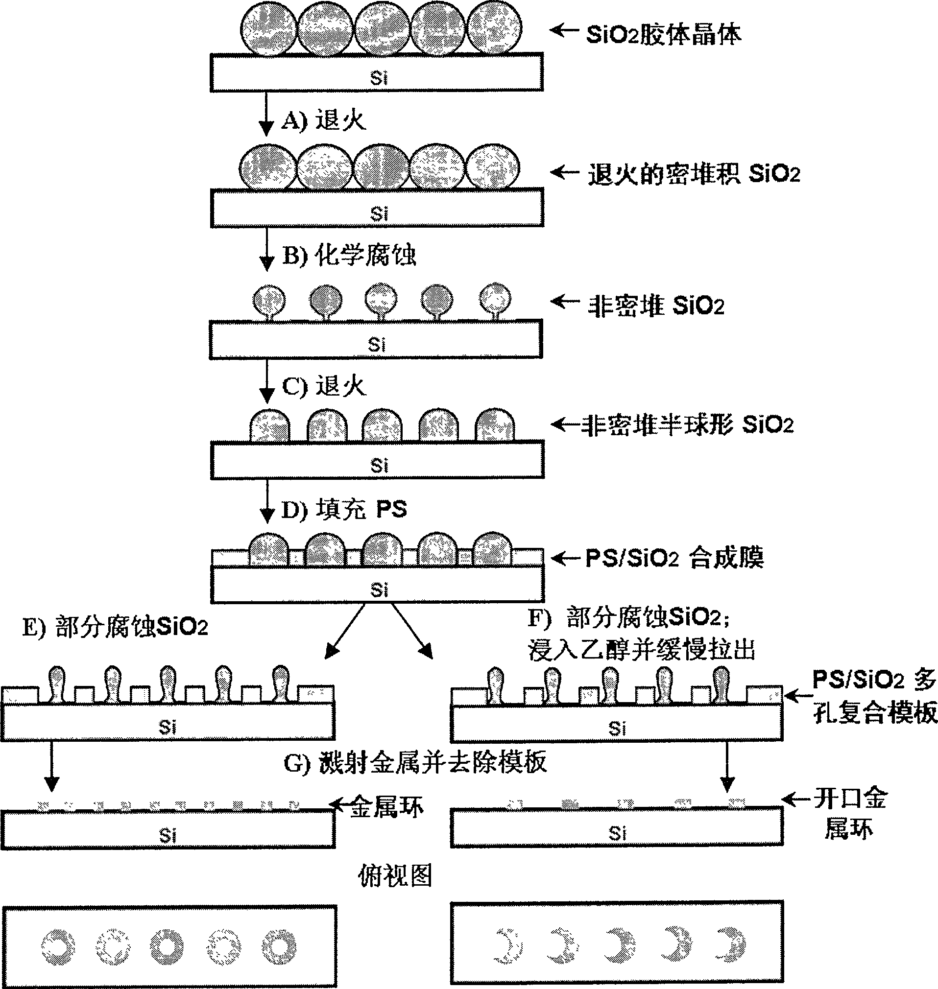
[0018] Example 1: The diameter of the selected micron / submicron silica microspheres is 1550nm (between 200nm and 10μm), the filled polymer is polystyrene (PS) (or other organic polymers), and the metal is sputtered The material is gold. The preparation method of two-dimensional ordered micron / sub-micron gold ring is:

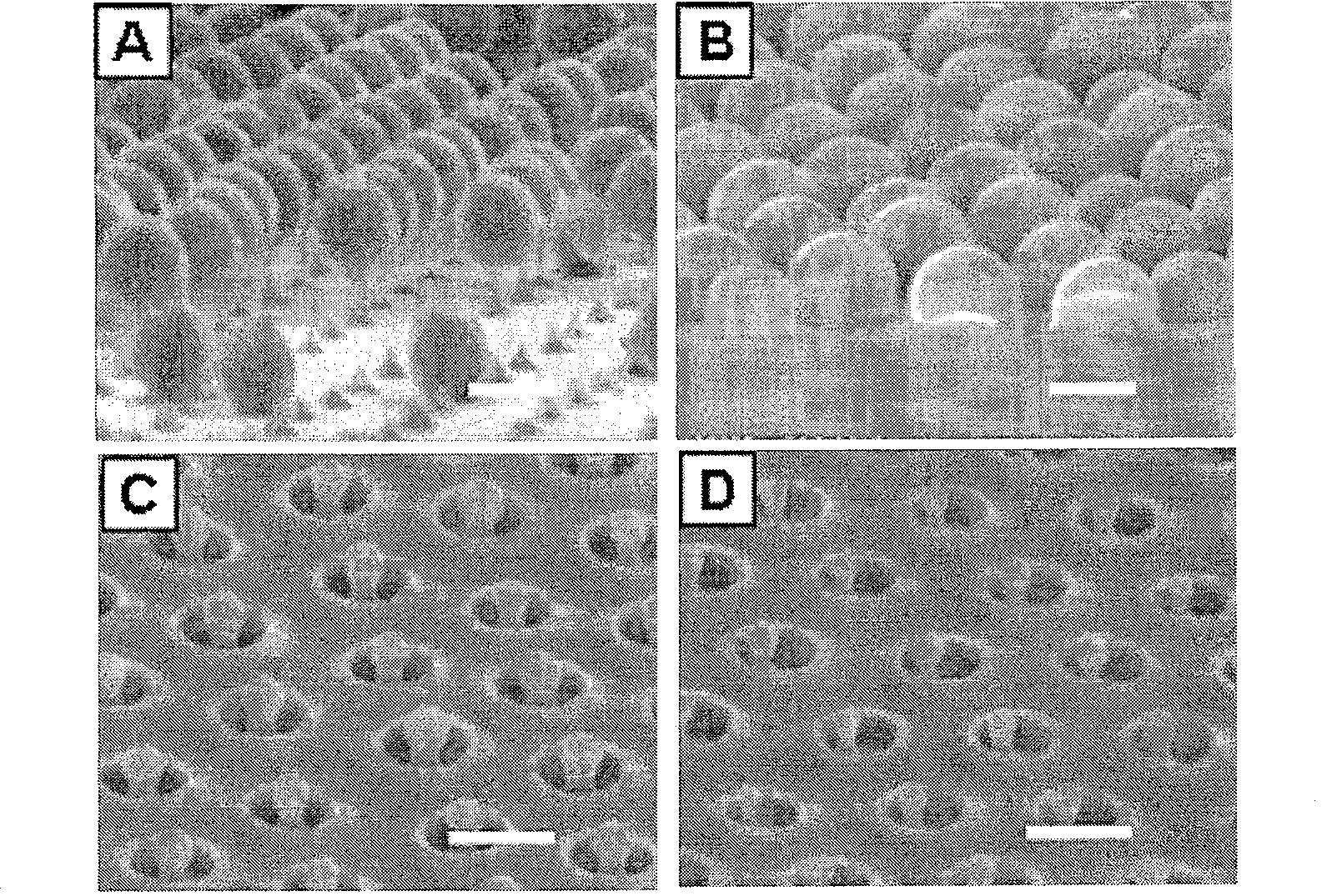
[0019] 1. Non-close-packed hemispherical SiO 2 Preparation of ordered arrays. Arrange SiO on silicon substrate by self-assembly technology 2 , To obtain a large area and highly ordered two-dimensional single-layer microsphere array; then after high temperature annealing at 1250℃ for 15min, 40% HF solution steam corrosion for 1~3.5min, to obtain non-close-packed SiO 2 Ordered array, see figure 2 (A); perform a second annealing at 1300℃ for 10 minutes to form a non-close-packed hemispherical SiO 2 Ordered array, see figure 2 (B), (the temperature of the high-temperature annealing treatment is 1250~1300℃, and the annealing time is within the range of 10~15min).

[00...

Embodiment 2

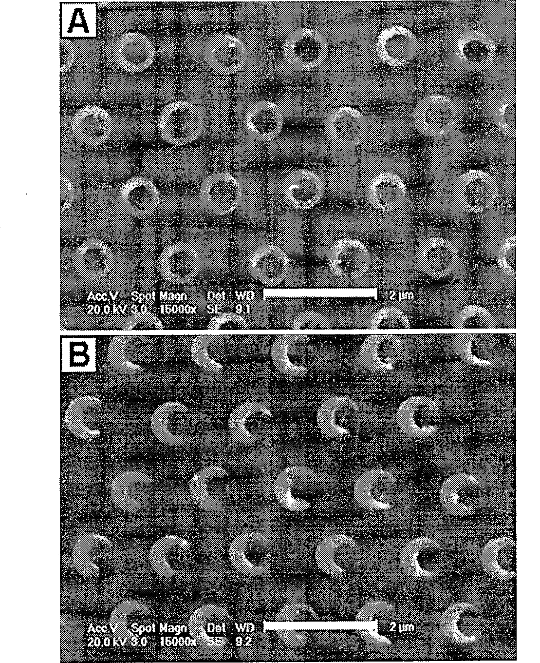
[0022] Example 2: Preparation of two-dimensional ordered micron / sub-micron gold split ring: The preparation process is basically the same as that of Example 1, but after obtaining PS / SiO 2 After the ring-shaped porous template is immersed in an alcohol solution, the template is slowly taken out at an angle. This process causes the PS porous membrane to move slightly until the boundary of the PS pore touches the SiO in the pore 2 , Thus obtained the open ring PS / SiO 2 Porous template, see figure 2 (D); After sputtering gold on the template and removing the template by the same method as in Example 1, a hexagonal non-close-packed two-dimensional ordered micron / submicron gold split ring array is obtained, and the outer boundary of the split metal ring is a circle Shape, and the inner cavity is a U-shaped structure, see image 3 (B), the adjustable range of its size parameter is the same as that of Example 1.


PUM

PropertyMeasurementUnit
diameteraaaaaaaaaa
diameteraaaaaaaaaa
thicknessaaaaaaaaaa

Abstract

The invention discloses a preparing method of the micro / sub-micron ferrule and the open ferrule. It gets the two-dimensional colloid crystal by the self-organizing technology, then to anneal in high temperature, chemical corruption, the secondary anneal in high temperature to form the non close-packed two-dimensional structure; the polymer is filled into lattice space to form the compound film which is put in the hydrofluoric acid steam to go on the secondary corrosion and form the ring space; the surface of the compound module is spurted by metal, then to resolve the compound module to get the ferrule array structure. If the sample is dipped into the alcohol solution to make the ring space change the partiality ring space; then to spurt by metal and remove the compound module to get the open ferrule. The advance of the invention is: the structural parameter can be controlled; the inner and outer diameter of the ferrule and the open ring can be adjusted and the circle can be controlled; the single disperse character is good and the thickness is uniform; the interface is clear and the technology is simple.

Description

Technical field [0001] The invention relates to a preparation method of a two-dimensional ordered micron / submicron metal ring and an artificial magnetic specific material formed by a two-dimensional ordered array of micron / submicron open metal rings. Background technique [0002] Two-dimensional ordered micron / submicron metal ring and split metal ring preparation technology is a technology with important application background. Due to the novel electromagnetic properties such as the adjustable plasmon resonance of the micron / submicron metal ring and the magnetic response of the micron / submicron open metal ring, the micron / submicron metal ring and the open ring are used in optical devices, high-density storage, and negative Refractive materials and other fields have potential applications. The current methods for preparing micron / submicron metal rings and split rings mainly include photolithography, electron beam or ion beam etching, focused ion beam direct writing, micro-contact ...

Claims


Application Information

Patent Timeline
Patent Type & Authority Patents(China)
IPC IPC(8): B81B1/00
Inventor 孟涛祝名伟潘剑唐超军詹鹏王振林闵乃本
Owner NANJING UNIV
Learn More