Organic ultraviolet optical sensor based on phosphorescence material light diode
A photovoltaic diode and organic ultraviolet light technology, which is applied in the field of organic ultraviolet light optical sensors, can solve the problems of high cost, complicated preparation process, and low response sensitivity, and achieve the effect of light weight, small volume, and high sensitivity
- Summary
- Abstract
- Description
- Claims
- Application Information
AI Technical Summary
Problems solved by technology
Method used
Image
Examples
Embodiment 1
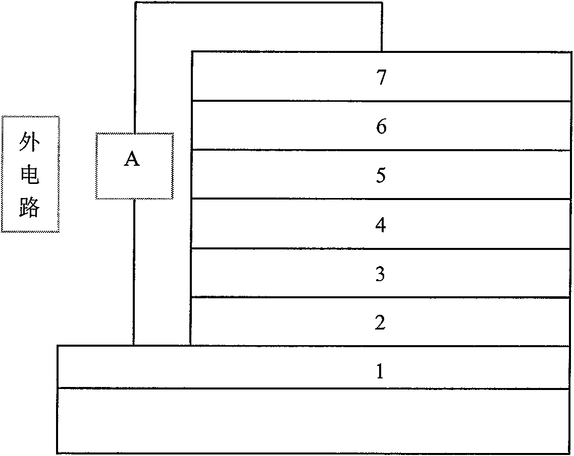
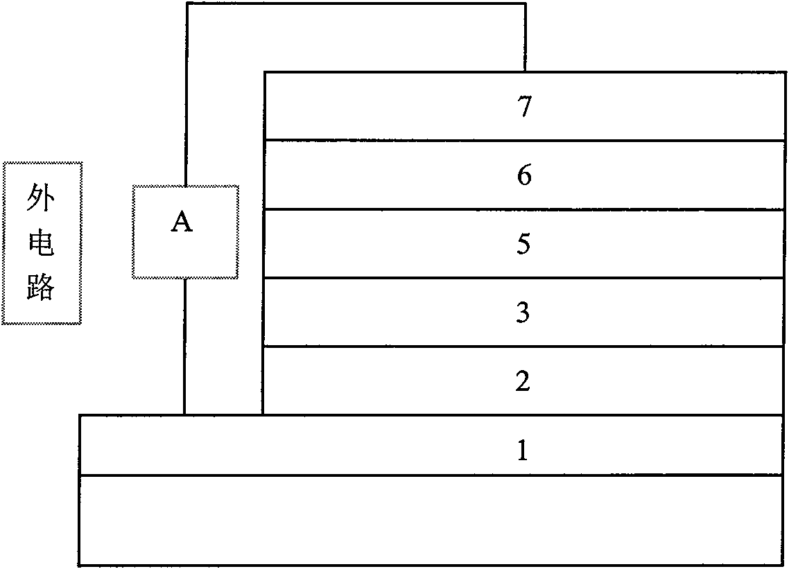
[0024] select figure 1 The device structure shown: In this embodiment, firstly, the hole-collecting electrode layer 2 selects the ITO film on the glass substrate 1 as the transparent conductive film. After cleaning the transparent conductive film on the substrate 1, at first in high vacuum (3-2 * 10 -1 Pascal), on the transparent conductive film, deposit one deck thickness and be 10nm electron donor layer 3, the material of electron donor layer 3 adopts TPD; Then on the electron donor layer 3, deposit the mixed layer of electron donor and electron acceptor 4. The thickness is 5nm, the electron donor material is TPD, and the electron acceptor material is Ir(ppy) 3 , TPD and Ir(ppy) 3 The weight ratio of the electron acceptor layer 5 is 1: 1; the electron acceptor layer 5 is deposited on the mixed layer 4 of the electron donor and the electron acceptor, and the material of the electron acceptor layer 5 is Ir (ppy) 3 , the thickness is selected as 20nm or 30nm or 40nm; after t...
Embodiment 2
[0026] The hole collecting electrode layer 2 selects the ITO film on the glass substrate 1 as a transparent conductive film, and the electron donor layer 3 selects m-MTDATA material with a thickness of 6nm; The mixed layer 4 of the acceptor has a thickness of 5nm, the material of the electron donor is m-MTDATA, and the material of the electron acceptor is Btp 2 Ir(acac), m-MTDATA and Btp 2 The weight ratio of Ir (acac) is 1: 1; Then deposit electron acceptor layer 5 on the mixed layer 4 of electron donor and electron acceptor, electron acceptor layer 5 selects material as Btp 2Ir (acac), the thickness is selected as 20nm or 30nm or 35nm; after that, an electron collection layer 6 is deposited on the electron acceptor layer 5, and the material of the electron collection layer 6 is LiF, and its thickness is 0.8nm; finally on the electron collection layer 6 The electron collecting electrode layer 7 is deposited, and the electron collecting electrode layer 7 is made of metal Al m...
Embodiment 3
[0029] The hole collecting electrode layer 2 selects the ITO film on the glass substrate 1 as a transparent conductive film; the electron donor layer 3 selects m-MTDATA material with a thickness of 15nm; the thickness of the mixed layer 4 of the electron donor and electron acceptor is 5nm, The electron donor material is m-MTDATA, and the electron acceptor is Ir(ppy) 3 , m-MTDATA and Ir(ppy) 3 The weight ratio is 1:1,; electron acceptor layer 5 selects Ir (ppy) 3 , the thickness is selected as 20nm or 25nm or 30nm; after that, an electron collection layer 6 is deposited on the electron acceptor layer 5, and the material of the electron collection layer 6 is LiF, and its thickness is 1.5nm; finally, an electron collection electrode is deposited on the electron collection layer 6 Layer 7, the electron collecting electrode layer 7 is made of metal Al, and its thickness is 120nm.
[0030] Adopt the measuring method described in embodiment 1 to measure result as follows:
[0031]...
PUM
 Abstract
Description
Claims
Application Information

