Micro fluid control chemistry sensor array chip using gel encapsule as base and preparing method
A chemical sensing and array chip technology, applied in the field of chemical sensing array chips, can solve the problems of low gel concentration requirements, difficult processing technology, unfavorable promotion and use, etc., to achieve wide application, reduce processing difficulty, and good sensing The effect of the characteristic
- Summary
- Abstract
- Description
- Claims
- Application Information
AI Technical Summary
Problems solved by technology
Method used
Image

Examples
Embodiment 1
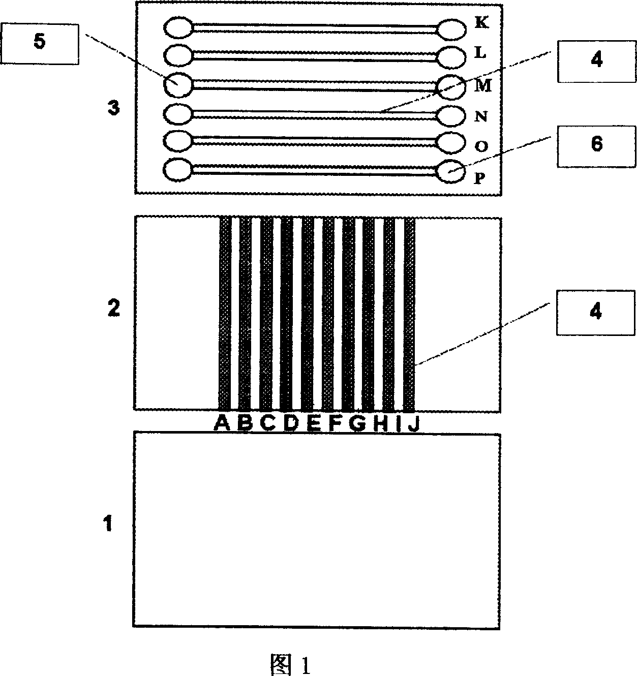
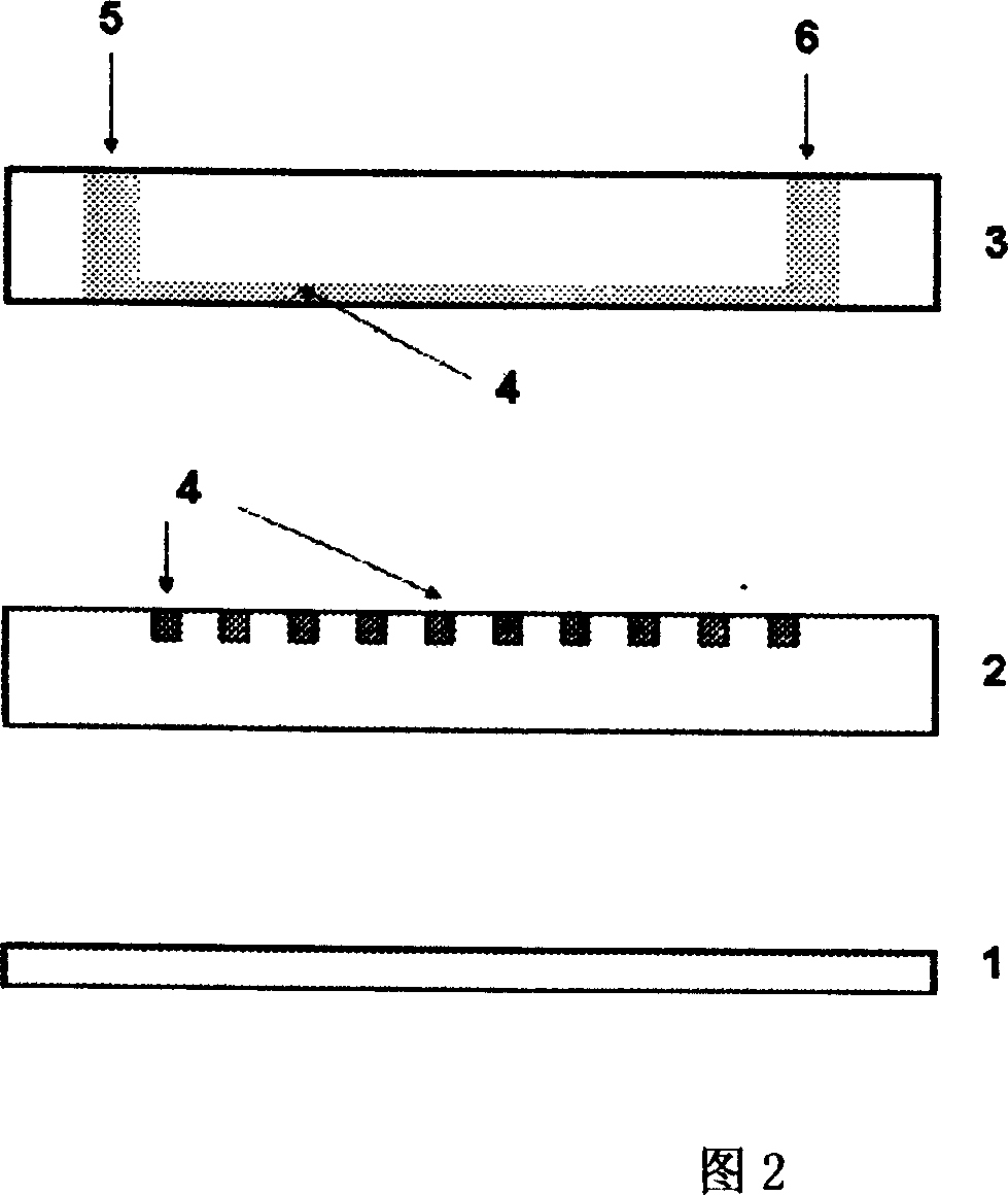
[0023] Referring to Figure 1 and Figure 2, the microfluidic chip is composed of three layers, the first layer is the carrier layer 1, made of glass, the second layer is the sensing array layer 2, and the third layer is the microfluidic channel layer 3, both layers are Made of PDMS. Layers II and III 2 and 3 have orthogonal microchannel networks 4, one for gel solidification and the other for sample flow. The microchannel network of layer II consists of ten parallel microfluidic channels A-J, and all channels in the microchannel network are filled with gel before combining with other layers. And the microchannel network of the third layer is composed of six parallel microfluidic channels K-P, which vertically intersect with the microchannels of the second layer 2 after the chip is combined. The two intersecting microchannel networks have a total of 60 intersections, and only at these specific intersections can the embedded gel be in contact with the sample solution flowing in ...
Embodiment 2
[0024] Embodiment 2: Utilize agarose gel to coat the calcium ion concentration of Fluo-3 sensing substance detection solution
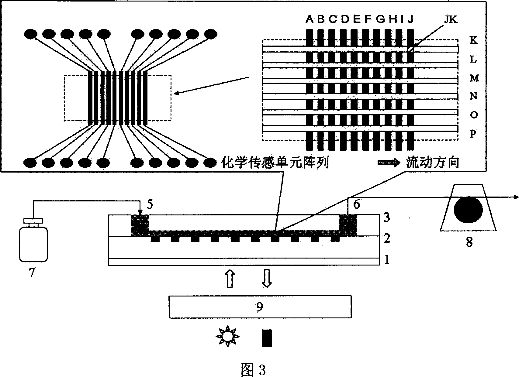
[0025] Fig. 3 is a schematic diagram of the structure of the detection device using this microfluidic chip. A rubber tube with an inner diameter of 1 mm is used to connect the inlet 5 and outlet 6 of the chip and fix it with a bracket. The sample solutions contained in the six reagent bottles 7 flow through different channels in the flow channel network driven by the micro-flow peristaltic pump 8 . At each intersection point, the calcium ions in the solution diffuse into the gel below, and react with the Fluo-3 molecules therein, and emit fluorescence under the irradiation of laser light. A laser confocal microscope 9 is used to detect the fluorescence intensity of each intersection point.
[0026] When the 1 μM calcium chloride solution flows through the microfluidic channel K, the fluorescence intensity at the intersection point JK (marked as the i...
Embodiment 3
[0028] Embodiment 3: The preparation method of the chemical sensing array layer, see Fig. 6:
[0029] Firstly, the positive relief master of the target channel structure is processed on the silicon wafer by photolithography-wet etching technology. Once the master is processed, it can be reused many times. The pattern in the master plate exactly matches the dimensions of the channels in the elastic rubber.
[0030] When the master plate is finished, the required channel network is machined on the elastic rubber by replica molding. Before the molding operation, the silicon mother board was washed with water and methanol in sequence, and then blown dry with nitrogen.
[0031] Degassed elastomeric rubber, here PDMS, polymer prepolymer (Sylgard 184 silicone rubber, Dow Corning, Midland, MI) and hardener were formulated in a 10:1 weight ratio and poured onto the silicon master. After vacuum removing air bubbles, the PDMS is solidified on the motherboard after hardening for at leas...
PUM
| Property | Measurement | Unit |
|---|---|---|
| Size | aaaaa | aaaaa |
Abstract
Description
Claims
Application Information
 - R&D
- Intellectual Property
- Life Sciences
- Materials
- Tech Scout
- Unparalleled Data Quality
- Higher Quality Content
- 60% Fewer Hallucinations
Browse by: Latest US Patents, China's latest patents, Technical Efficacy Thesaurus, Application Domain, Technology Topic, Popular Technical Reports.
© 2025 PatSnap. All rights reserved.Legal|Privacy policy|Modern Slavery Act Transparency Statement|Sitemap|About US| Contact US: help@patsnap.com