Method for producing electromagnetic wave shielding material
A shielding material, electromagnetic wave technology, applied in the fields of magnetic/electric field shielding, shielding, electrical components, etc., can solve the problem of high polymer film strength and release film thickness, difficult to obtain pressure-sensitive adhesive and protective film, and reduce production efficiency. and yield and other issues, to achieve the effect of inhibiting the pickling time from being too long, saving production processes and improving production efficiency.
- Summary
- Abstract
- Description
- Claims
- Application Information
AI Technical Summary
Problems solved by technology
Method used
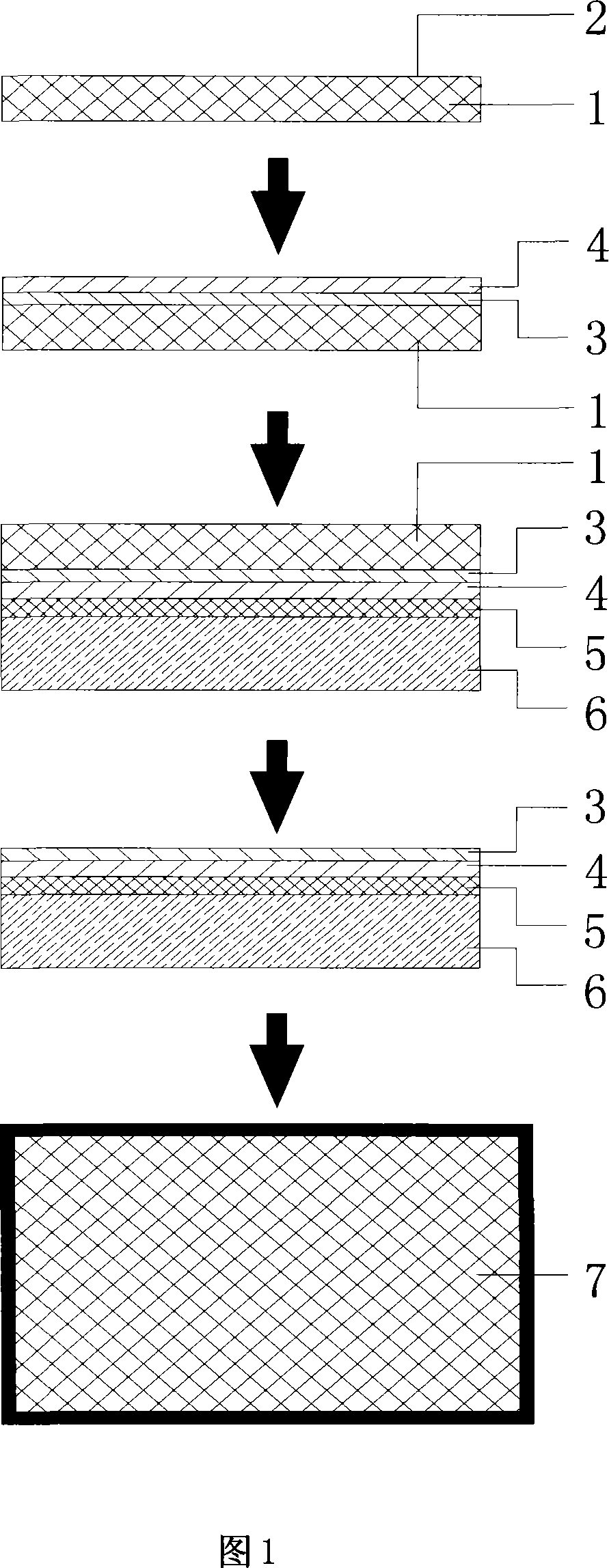
Image

Examples
Embodiment 1
[0051] On the polyester film (PET) surface with a length of 200 meters, a width of 1030mm, and a thickness of 75 microns, the surface pretreatment is carried out with plasma, and the surface dyne value is 20, and then vacuum magnetron sputtering copper plating is carried out on the treated surface. Vacuum degree is 2.5×10 -2 Pa, the moving speed of the polyester film is 1.5m / min, and the surface resistance of the material at this time is 100-150Ω / sq.
[0052] A thick metal copper layer of 5 μm is electroplated on the vacuum magnetron sputtering coating to produce a PET film copper-clad board.
[0053] Alkaline pyrophosphate copper plating conditions are as follows: plating solution contains copper pyrophosphate: 50g / L; potassium pyrophosphate: 300g / L; ammonium citrate: 20g / L; ammonia water: 3ml / L; pH value: 8.3; temperature: 45℃; current density: 1.0A / dm 2 ; Cathode moving speed: 5.0m / h, using air stirring, normal filtration, voltage 4V, the surface resistance of the materia...
Embodiment 2
[0057] The surface of the polyimide film (PI) with a length of 200 meters, a width of 1030 mm and a thickness of 50 microns is pretreated with plasma, and the surface dyne value is 20, and then vacuum magnetron sputtering nickel plating is carried out, and the vacuum degree is 2.1 ×10 -2 Pa, the moving speed of the polyimide film is 1.2m / min, and the surface resistance of the material at this time is 70-100Ω / sq.
[0058] A thick metal nickel layer of 10 μm is electroplated on the vacuum magnetron sputtering coating to produce a metallized PI film.
[0059] Acidic nickel plating conditions: nickel sulfate: 200g / L; nickel chloride: 40g / L; boric acid: 30g / L; pH value: 4.0; temperature: 40°C; current density: 5A / dm 2 ; Cathode moving speed: 8.0m / h, using air stirring, normal filtration, voltage 4V. At this time, the surface resistance of the material was 0.010Ω / sq.
[0060] The above-mentioned metal nickel layer was pasted on the plexiglass with a thickness of 5 mm and a light ...
Embodiment 3
[0063] The surface of the polyethylene film with a length of 200 meters, a width of 1030 mm and a thickness of 125 microns is pretreated with plasma, and the surface dyne value is 22, and then vacuum magnetron sputtering is carried out to plate copper and nickel, and the vacuum degree is 2.2×10 -2 Pa, the moving speed of the polyethylene film is 2.0m / min, and the surface resistance of the material at this time is 150-200Ω / sq.
[0064] On the vacuum magnetron sputtering coating, a 1.5 μm copper layer is first electroplated, and then a 0.1 μm metallic nickel (protective copper layer) is electroplated, thus producing a polyethylene film copper-plated with nickel.
[0065] Alkaline pyrophosphate copper plating conditions are as follows: plating solution contains copper pyrophosphate: 50g / L; potassium pyrophosphate: 300g / L; ammonium citrate: 20g / L; ammonia water: 3ml / L; pH value: 8.3; temperature: 45℃; current density: 1.0A / dm 2 ; Cathode moving speed: 10.0m / h, using air stirring,...
PUM
| Property | Measurement | Unit |
|---|---|---|
| Thickness | aaaaa | aaaaa |
| Thickness | aaaaa | aaaaa |
| Thickness | aaaaa | aaaaa |
Abstract
Description
Claims
Application Information
 - Generate Ideas
- Intellectual Property
- Life Sciences
- Materials
- Tech Scout
- Unparalleled Data Quality
- Higher Quality Content
- 60% Fewer Hallucinations
Browse by: Latest US Patents, China's latest patents, Technical Efficacy Thesaurus, Application Domain, Technology Topic, Popular Technical Reports.
© 2025 PatSnap. All rights reserved.Legal|Privacy policy|Modern Slavery Act Transparency Statement|Sitemap|About US| Contact US: help@patsnap.com