Method for developing m-face or a-face ZnO film by metal organic chemical vapour deposition
A metal organic chemistry and vapor deposition technology, applied in gaseous chemical plating, metal material coating process, coating and other directions, can solve problems such as difficulty in meeting industrialization needs, and achieve the effect of wide industrial application prospects
- Summary
- Abstract
- Description
- Claims
- Application Information
AI Technical Summary
Problems solved by technology
Method used
Image
Examples
Embodiment 1
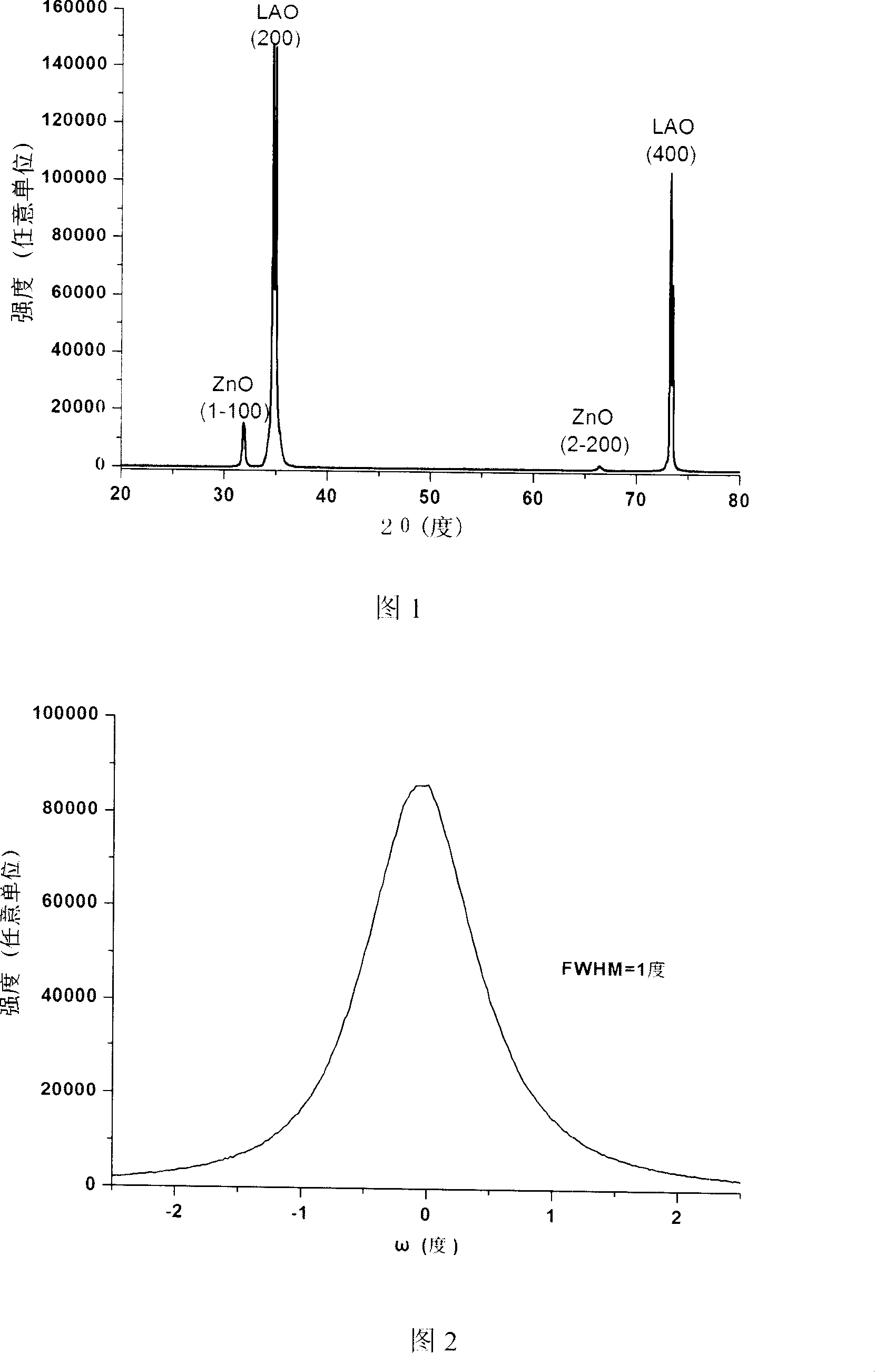
[0022] Example 1 LiAlO on (200) plane 2 m-plane ZnO epitaxial films grown on
[0023] The specific growth steps are as follows:
[0024] 1. Cleaning of the substrate wafer. The polished (200) surface LiAlO 2 Put the wafer into a beaker filled with acetone, ultrasonically clean it at 20°C for 10 minutes, and then take out the wafer and soak it in absolute ethanol for 10 minutes. During the whole cleaning process, avoid direct contact with the wafer with your hands.
[0025] 2. Growth. The cleaned (200) surface γ-LiAlO 2 The single crystal substrate is placed in the growth chamber of the LP-MOCVD system. The reaction process uses diethyl zinc (DEZn) as the zinc source, and high-purity oxygen (O 2 ) as the oxygen source, and high-purity argon (Ar) as the carrier gas and diluent gas of the saturated vapor of the zinc source. Diethylzinc (DEZn) bubbler conditions were maintained at 760 Torr, 14°C. Zinc source flow is 20sccm, O 2 The gas flow is 120 sccm, the Ar gas flow is ...
Embodiment 2
[0030] Example 2 In (302) LiAlO 2 a-plane ZnO epitaxial film grown on
[0031] Using LiAlO on the (200) plane as above 2 The same process parameters for growing m-plane ZnO epitaxial films on (302)LiAlO 2 a-plane ZnO films were grown on them.
[0032] The thin film prepared in embodiment 2 has been characterized, and the results are explained as follows:
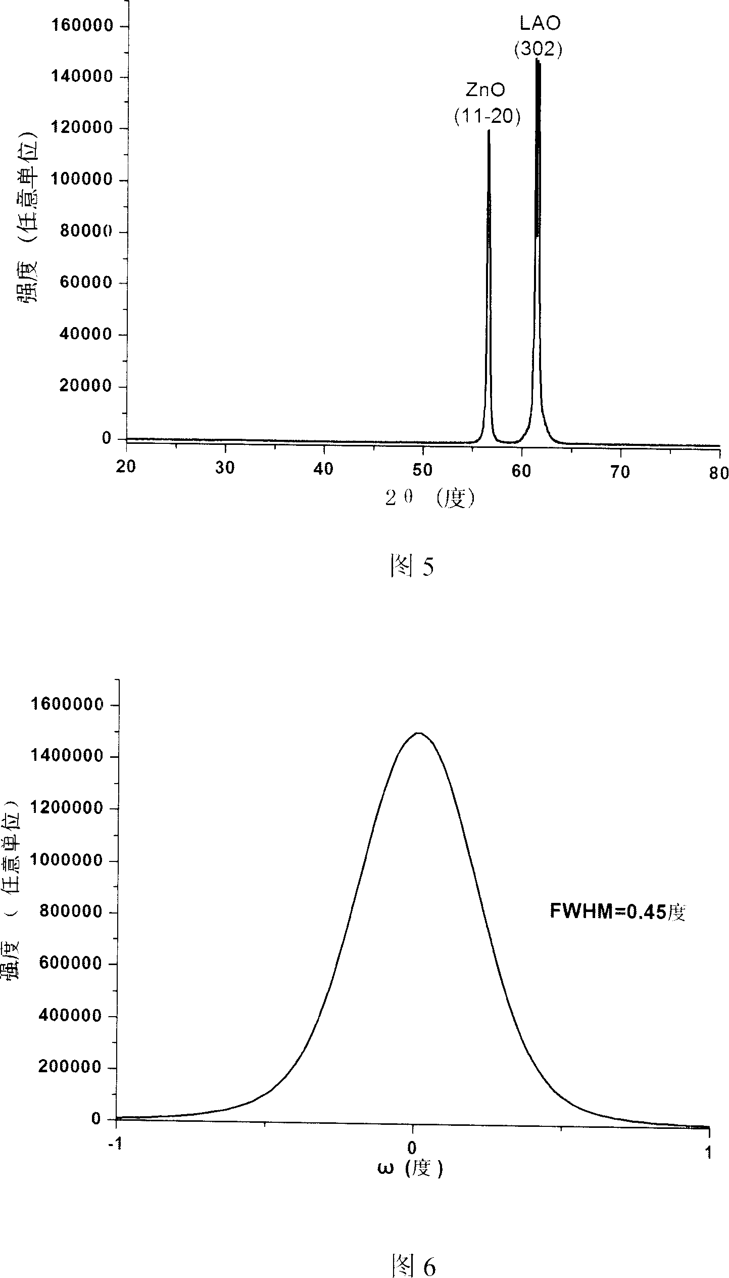
[0033] Fig. 5 is the XRD spectrum of the sample of Example 2.
[0034] Figure 5 is the XRD pattern of the prepared sample. γ-LiAlO 2 The diffraction peak of the substrate (302) crystal plane is at 61.37°; the peak of a-plane ZnO is at 56.53°. Fig. 6 is the rocking curve of the sample of Example 2, and its full width at half maximum FWHM=0.45°.
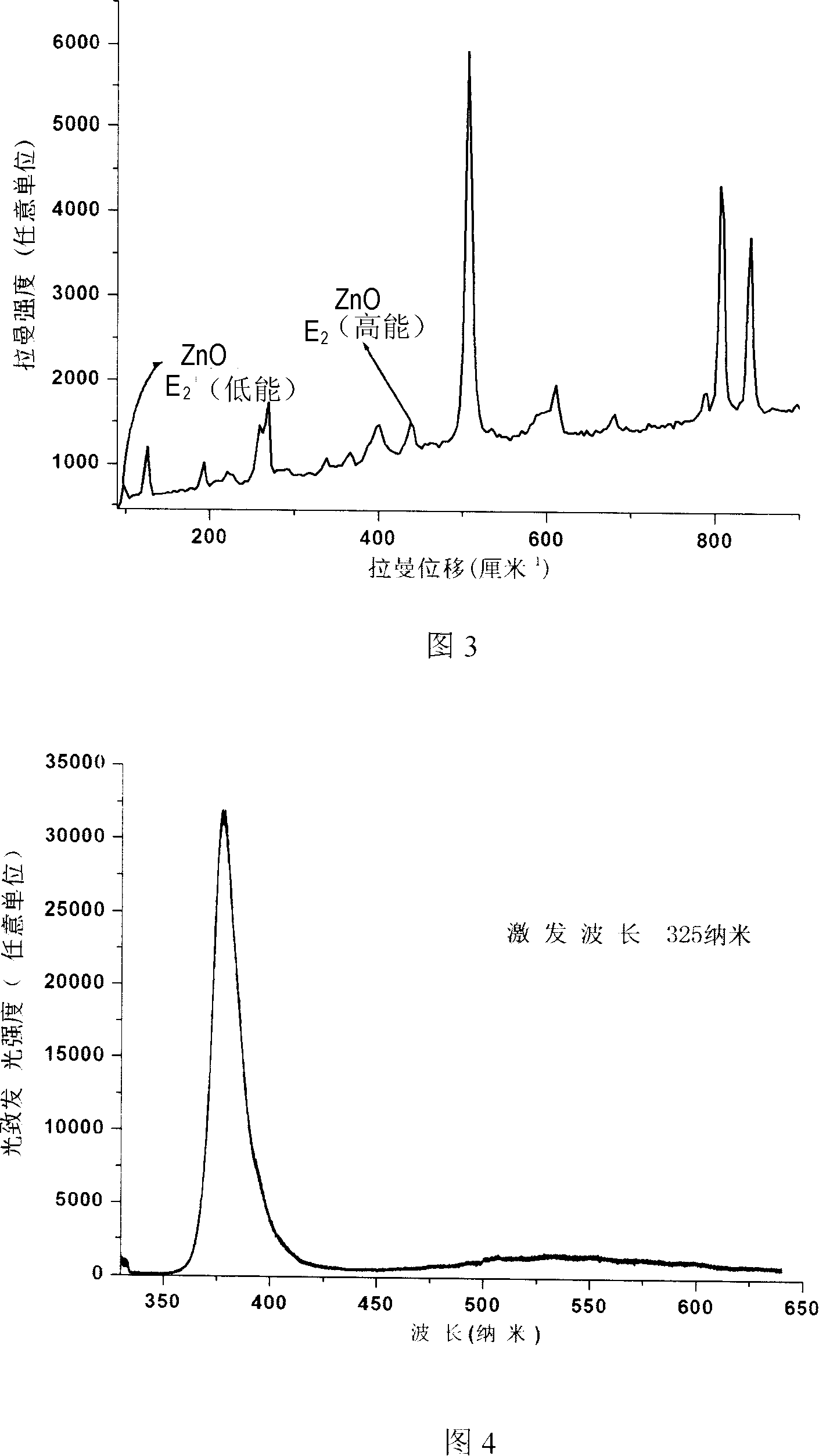
[0035] Fig. 7 is the laser Raman scattering pattern of the sample of embodiment 2, all have very strong ZnO lattice vibration signal in the sample, and wherein wavenumber is 97.6cm -1 The characteristic peaks of ZnO correspond to the low-energy E 2 modes of vibration, while ...
PUM
 Abstract
Description
Claims
Application Information
 - R&D
- Intellectual Property
- Life Sciences
- Materials
- Tech Scout
- Unparalleled Data Quality
- Higher Quality Content
- 60% Fewer Hallucinations
Browse by: Latest US Patents, China's latest patents, Technical Efficacy Thesaurus, Application Domain, Technology Topic, Popular Technical Reports.
© 2025 PatSnap. All rights reserved.Legal|Privacy policy|Modern Slavery Act Transparency Statement|Sitemap|About US| Contact US: help@patsnap.com


