ZnO based LED and its preparing process
A technology of light-emitting diodes and electrodes, which is applied to electrical components, circuits, semiconductor devices, etc., can solve the problems that the performance of p-type ZnO thin films needs to be improved, the growth conditions are difficult to control, and the equipment maintenance is difficult, so as to improve the repeatability and growth cost. low, the effect of improving device performance
- Summary
- Abstract
- Description
- Claims
- Application Information
AI Technical Summary
Problems solved by technology
Method used
Image

Examples
Embodiment 1
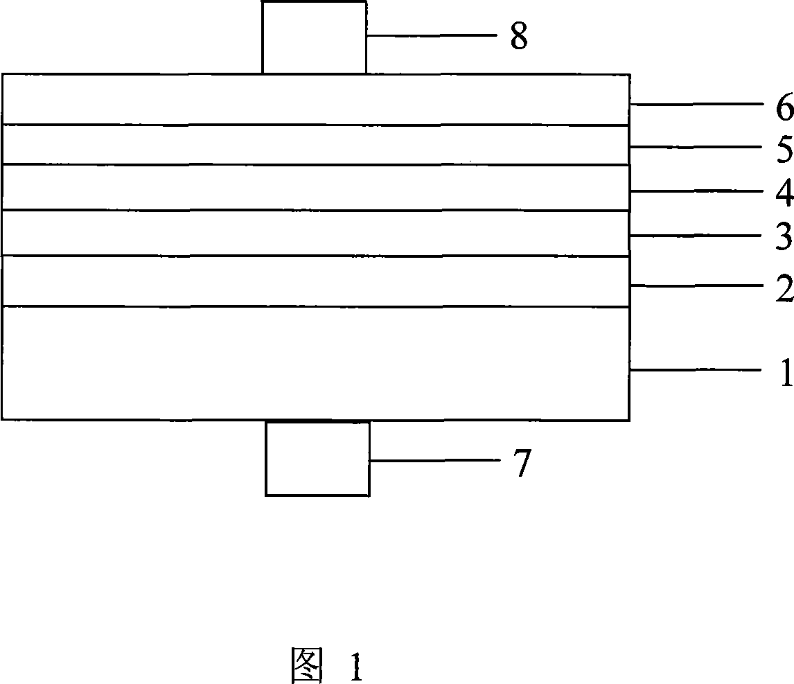
[0017] Clean the surface of the silicon substrate and put it into the growth chamber of the metal-organic chemical vapor deposition system, and the growth chamber is evacuated to 10 -4 pa, heat the substrate to 500°C, feed organic zinc source and oxygen, and deposit n-ZnO film layer on one side of the substrate with Ga as the dopant source, the growth pressure is 50Torr, and the film thickness is 2μm; then feed organic zinc Source, organic magnesium source, oxygen, the growth pressure is 50Torr, deposit n-Zn on the n-ZnO film layer 0.8 Mg 0.2 O thin film layer, the thickness of the film layer is 50nm; then alternately feed organic zinc source, oxygen and organic zinc source, organic magnesium source, oxygen, the growth pressure is 50Torr, deposit ZnO layer and Zn 0.9 Mg 0.1 O layer, forming 5 cycles of ZnO / Zn 0.9 Mg 0.1 O quantum well layer, ZnO and Zn 0.9 Mg 0.1 The O widths are 5nm and 6nm respectively; then lower the temperature to 400°C and feed organic zinc source, ...
Embodiment 2
[0019] Clean the surface of the zinc oxide substrate and put it into the growth chamber of the metal organic chemical vapor deposition system, and the growth chamber is evacuated to 10 -4 Pa, heat the substrate to 550°C, feed organic zinc source and oxygen, and deposit n-ZnO film layer on one side of the substrate with Ga as the dopant source, the growth pressure is 50 Torr, and the film thickness is 1.5 μm; Zinc source, organic magnesium source, oxygen, growth pressure of 50Torr, deposit n-Zn on the n-ZnO film layer 0.75 Mg 0.25 O film layer, the thickness of the film layer is 50nm; then alternately feed organic zinc source, oxygen and organic zinc source, organic magnesium source, oxygen, the growth pressure is 50 Torr, deposit ZnO layer and Zn 0.8 Mg 0.2 O layer, forming 7 periods of ZnO / Zn 0.8 Mg 0.2 O quantum well layer, ZnO and Zn 0.8 Mg 0.2 The O widths are 5nm and 5nm respectively; then lower the temperature to 400°C and feed organic zinc source, organic magnesiu...
Embodiment 3
[0021] Clean the gallium nitride substrate surface and put it into the growth chamber of the metal-organic chemical vapor deposition system, and the growth chamber is evacuated to 10 -4 Pa, heat the substrate to 600°C, feed organic zinc source and oxygen, and deposit n-ZnO film layer on one side of the substrate with Al as the doping source, the growth pressure is 50Torr, and the film thickness is 2μm; then feed organic zinc Source, organic magnesium source, oxygen, the growth pressure is 50Torr, deposit n-Zn on the n-ZnO film layer 0.5 Mg 0.5 O film layer, the thickness of the film layer is 30nm; then alternately feed organic zinc source, oxygen and organic zinc source, organic magnesium source, oxygen, the growth pressure is 50Torr, deposit ZnO layer and Zn 0.6 Mg 0.4 O layer, forming 10 cycles of ZnO / Zn 0.6 Mg 0.4 O quantum well layer, ZnO and Zn 0.6 Mg 0.4 The O widths are 4nm and 4nm respectively; then lower the temperature to 400°C and feed organic zinc source, org...
PUM
 Abstract
Description
Claims
Application Information
 - R&D
- Intellectual Property
- Life Sciences
- Materials
- Tech Scout
- Unparalleled Data Quality
- Higher Quality Content
- 60% Fewer Hallucinations
Browse by: Latest US Patents, China's latest patents, Technical Efficacy Thesaurus, Application Domain, Technology Topic, Popular Technical Reports.
© 2025 PatSnap. All rights reserved.Legal|Privacy policy|Modern Slavery Act Transparency Statement|Sitemap|About US| Contact US: help@patsnap.com