

Corrosion resistant wafer processing apparatus and method for making thereof
A processing equipment, wafer processing technology, applied in semiconductor/solid-state device manufacturing, coating, gaseous chemical plating, etc., can solve problems such as easy cracks, short service life, limited thermal slope, etc.
- Summary
- Abstract
- Description
- Claims
- Application Information
AI Technical Summary
Problems solved by technology
Method used
Image

Examples
example 1
[0108] Example 1: In this example, the glass was prepared from a homogeneous powder mixture of reactant grade raw materials in amounts of 45 wt% yttrium oxide, 20 wt% alumina, and 35 wt% silica. The powder mixture was melted at 1400°C for 1 hour in a platinum crucible. The glass melt was poured into a steel mold and annealed from 680°C to room temperature for 12 hours. Utilize Al 2 o 3 Element's Mill crushed and ground each glass in propanol to form a glass frit composition having an average particle size of 100 μm.
[0109] In the next step, glass powder was added to the colloidal alumina solution in an amount of 75 wt.% glass powder and 25 wt.% colloidal alumina to form a glass-ceramic bonding glue / adhesive. Colloidal alumina solutions are commercially available from Nycaol Nano Technologies as Nyacol(R) AL20DW, containing 20-25 wt. Al in 75-79 wt.% distilled water 2 o 3 , 1000°C to form an etchant resist layer that protects the underlying components. The high temper...
example 2
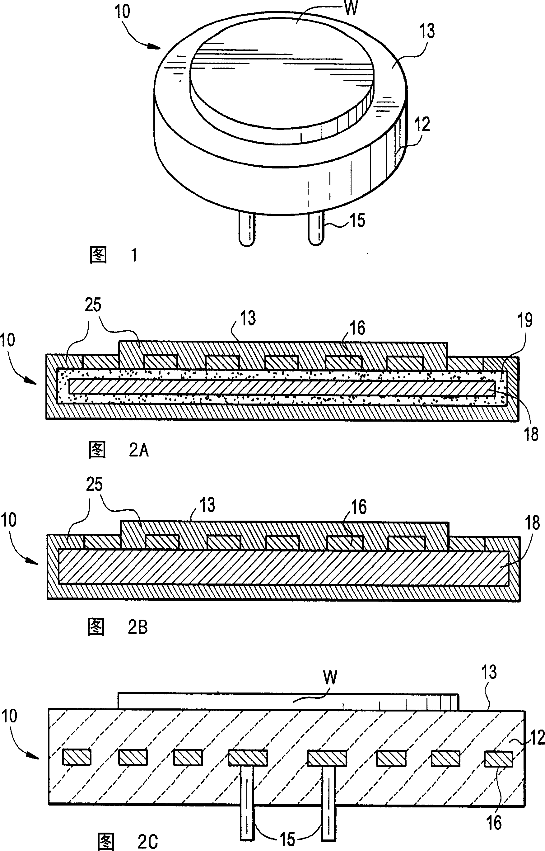
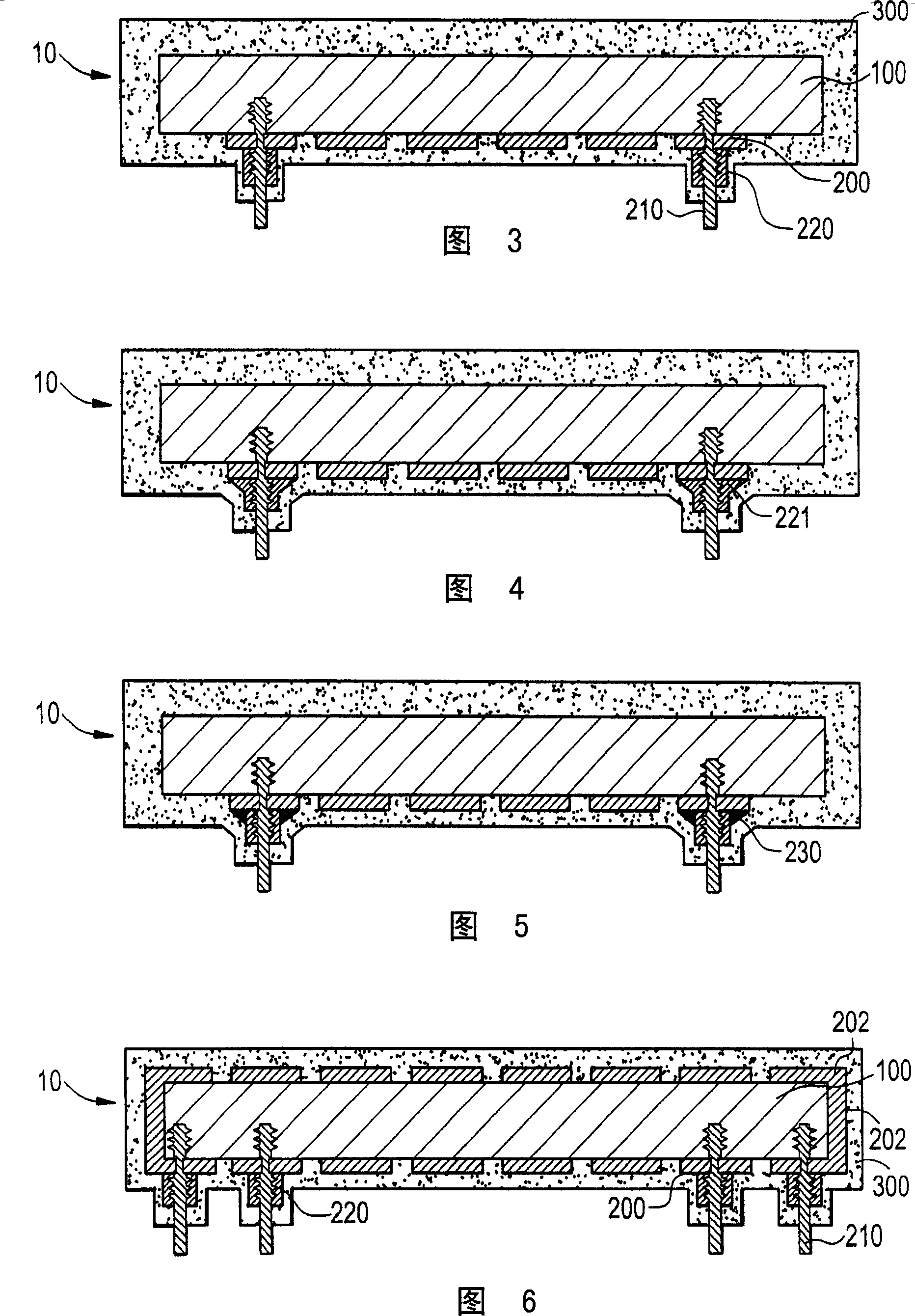
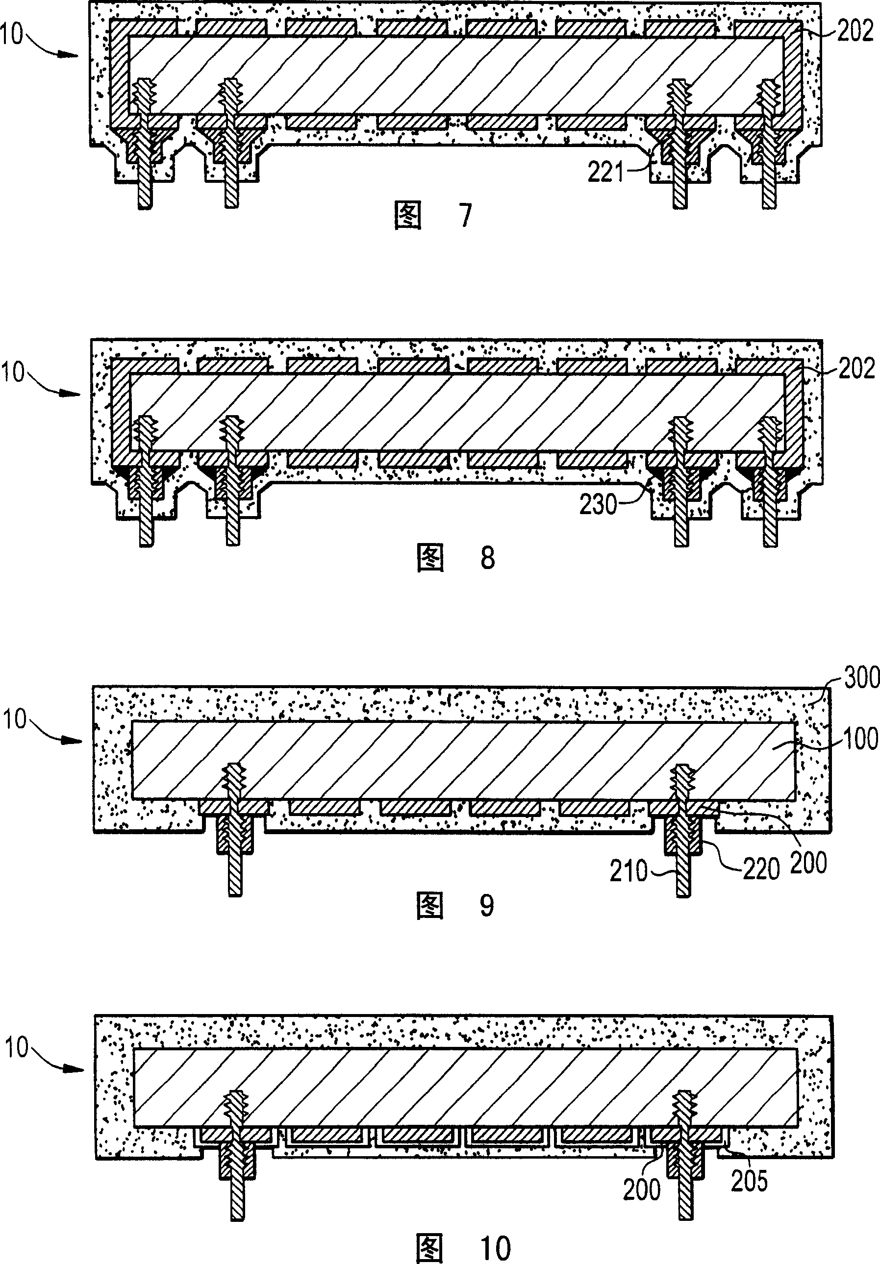
[0110] Example 2: The conductive heating element (MoMn) is deposited on a ceramic substrate (AlN). The substrate includes through holes to allow electrical contacts to be mounted. In the next step, install the Ni-plated molybdenum posts using molybdenum fasteners. The adhesive of Example 1 was painted around the contact points between the Ni-plated molybdenum posts, molybdenum fasteners, heating elements and the AlN substrate on the AlN substrate. Next, the entire heating assembly including contacts is coated with AlN by a CVD process.
[0111] Corrosion tests of heaters and contacts were performed after 100 thermal cycles between 400 and 500 °C with a ramp rate of 45 °C / min under test simulation conditions for heaters with AlN substrates in a semiconductor processing environment. In another test, a heater with a graphite core was cycled 100 times between 400 and 600°C with a ramp rate of 60°C / min. Test to determine whether glass-ceramic adhesives perform adequately under...
example 3
[0114] Example 3: Filler compositions comprising powder mixtures of reactant grade feedstocks ranging from 45 wt% yttrium oxide, 20 wt% alumina, 35% wt% silica were compared to other materials known in the art including alumina, molybdenum, TaC, AlN, graphite and nickel. In this test, a) the size and mass of the sample is measured prior to testing; b) the part is placed in a vacuum chamber, which is then pumped to a pressure of approximately 1 millitorr; c) the part is heated to the desired Test temperature; d) Generate a fluorine / argon plasma over the part for the desired period of time; e) After testing, remove the part from the chamber and record the mass after exposure. The corrosion rate is calculated as follows:
[0115] Corrosion rate = mass loss / density / exposed surface area / time;
[0116] Where a negative etch rate represents a mass gain after exposure, which translates into good corrosion resistance.
PUM
| Property | Measurement | Unit |
|---|---|---|
| etch rate | aaaaa | aaaaa |
| etch rate | aaaaa | aaaaa |
| thickness | aaaaa | aaaaa |
Abstract
Description
Claims
Application Information