Gallium-adulterated Ga3Sb8Te1 phase change memory unit and its making method
A technology of phase-change storage and phase-change materials, which is applied in the field of gallium-doped Ga3Sb8Te1 phase-change memory cells and its preparation, devices and its preparation. Problems such as storage unit and embedded phase-change storage unit technical solutions are not given, achieving high thermal stability, erasable cycle times, and erased times.
- Summary
- Abstract
- Description
- Claims
- Application Information
AI Technical Summary
Problems solved by technology
Method used
Image
Examples
Embodiment 1
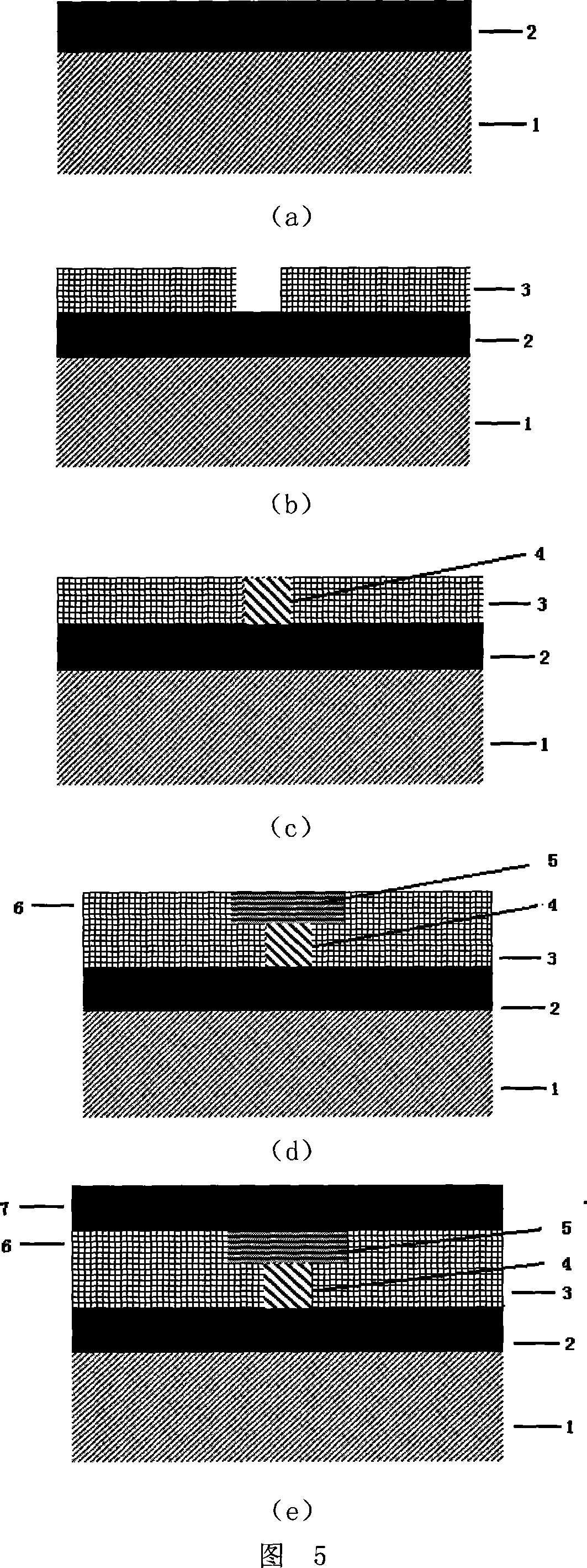
[0042] The above-mentioned gallium-doped phase-change memory cell based on the present invention, in conjunction with accompanying drawing 5, its preparation steps are as follows:
[0043] The first step is to deposit a layer of lower electrode material TiW on the silicon substrate by magnetron sputtering, with a thickness of 150nm, a melting point of 1750°C, and a thermal conductivity of 1.7J / cm-k-s, as shown in the attached figure 5(a).
[0044] In the second step, a layer of SiO is deposited on the lower electrode material of the first step by CVD (chemical vapor deposition). 2 The insulating dielectric layer has a thickness of 150nm and a thermal conductivity of 0.014J / cm-k-s. Then, through nanoimprint lithography and dry etching technology, a small hole is carved in the center of the insulating dielectric layer, the diameter of the small hole is 20nm, and the depth is 30nm, as shown in Figure 5(b).
[0045] In the third step, the magnetron sputtering method is used to f...
Embodiment 2
[0050] The above-mentioned gallium-doped phase-change memory cell based on the present invention, in conjunction with accompanying drawing 5, its preparation steps are as follows:
[0051] The first step is to deposit a layer of PtW alloy as the lower electrode material on the silicon substrate by magnetron sputtering, with a thickness of 150nm, a melting point of 1800°C, and a thermal conductivity of 2.0J / cm-k-s, as shown in the attached Figure 5(a).
[0052] In the second step, a layer of SiO is deposited on the lower electrode material of the first step by CVD (chemical vapor deposition). 2 The insulating dielectric layer has a thickness of 250nm and a thermal conductivity of 0.014J / cm-k-s. Then, by nanoimprint lithography and dry etching technology, a small hole is carved in the center of the insulating dielectric layer, the diameter of the small hole is 20nm, and the depth is 100nm, as shown in Figure 5(b).
[0053] In the third step, the magnetron sputtering method is ...
Embodiment 3
[0058] The above-mentioned gallium-doped phase-change memory cell based on the present invention, in conjunction with accompanying drawing 5, its preparation steps are as follows:
[0059] The first step is to deposit a layer of lower electrode material TiW on the silicon substrate by magnetron sputtering, with a thickness of 150nm, a melting point of 1780°C, and a thermal conductivity of 1.76J / cm-k-s, as shown in the attached figure 5(a).
[0060] In the second step, a layer of SiO is deposited on the lower electrode material of the first step by evaporation. 2 The dielectric insulating dielectric layer has a thickness of 200nm and a thermal conductivity of 0.014J / cm-k-s. Then, through nanoimprint lithography and dry etching technology, a small hole is carved in the center of the insulating dielectric layer, the diameter of the small hole is 20nm, and the depth is 50nm, as shown in Figure 5(b).
[0061] In the third step, the magnetron sputtering method is used to fill the ...
PUM
| Property | Measurement | Unit |
|---|---|---|
| Thickness | aaaaa | aaaaa |
| Melting point | aaaaa | aaaaa |
| Thickness | aaaaa | aaaaa |
Abstract
Description
Claims
Application Information


