GaN thin film upgrowth method based on Al3O2 substrate

A thin film growth and substrate technology, applied in the direction of gaseous chemical plating, lasers, coatings, etc., can solve the problem of limiting the performance of GaN-based microwave high-power transistors, light-emitting diodes and lasers, and reducing the crystallization quality and critical thickness and temperature of the GaN top layer The problems such as large up and down changes can be achieved to reduce the influence of thermal stress, reduce the density of linear dislocations, and reduce the effect of surface cracks

Inactive Publication Date: 2008-03-12
XIDIAN UNIV
View PDF0 Cites 21 Cited by
  • Summary
  • Abstract
  • Description
  • Claims
  • Application Information

AI Technical Summary

Problems solved by technology

However, this method of using a low-temperature insertion layer, due to the large temperature rise and fall during the film growth process, produces excessive thermal stress, reduc

Method used


Image

  • GaN thin film upgrowth method based on Al3O2 substrate
  • GaN thin film upgrowth method based on Al3O2 substrate
  • GaN thin film upgrowth method based on Al3O2 substrate

Examples


Embodiment 1

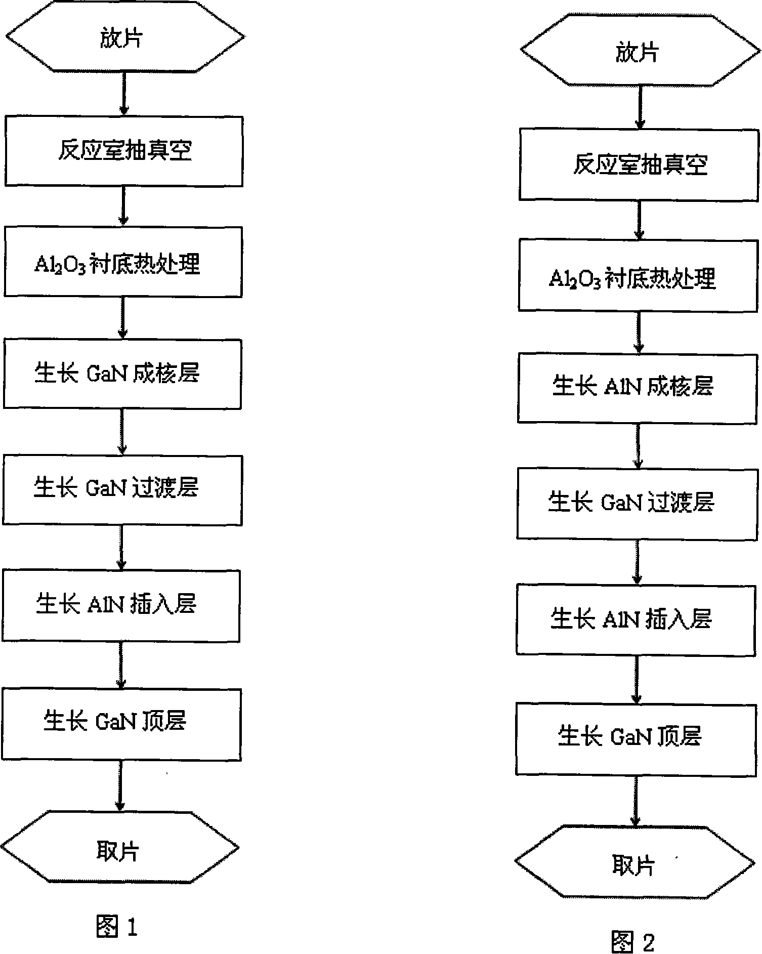
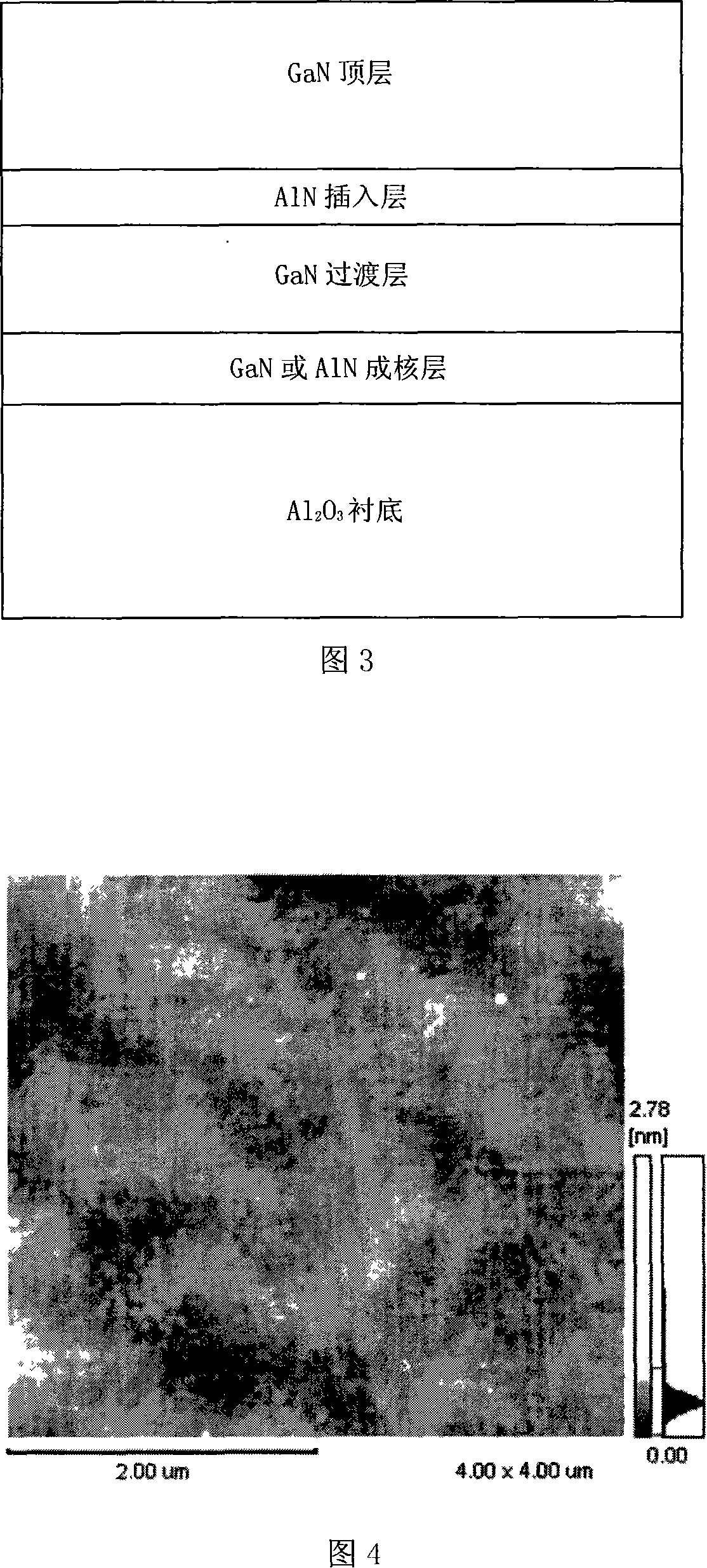
[0034] Referring to Figure 1, in Al 2 o 3 Using GaN as the nucleation layer material on the substrate to grow a GaN film with a high-temperature AlN insertion layer, the specific steps are as follows:

[0035] 1. Take Al 2 o 3 The substrate is placed in the reaction chamber of the metal organic chemical vapor deposition equipment MOCVD, and the vacuum degree of the reaction chamber is pumped to 1×10 -2 Under Torr, under the protection of the mixed gas of hydrogen and ammonia, Al 2 o 3 The substrate is heat-treated, the heating temperature is 1050°C, the heating time is 5min, the pressure of the reaction chamber is 40Torr, the flow rate of hydrogen gas is 1500 sccm, and the flow rate of ammonia gas is 1500 sccm;

[0036] 2. Lower the substrate temperature to 500°C, keep the growth pressure at 40Torr, the flow rate of hydrogen gas at 1500sccm, the flow rate of ammonia gas at 1500sccm, and feed a gallium source with a flow rate of 30μmol / min into the reaction chamber to grow...

Embodiment 2

[0041] Referring to Figure 1, in Al 2 o 3 Using GaN as the nucleation layer material on the substrate to grow a GaN film with a high-temperature AlN insertion layer, the specific steps are as follows:

[0042] 1. Take Al 2 o 3 The substrate is placed in the reaction chamber of metal organic chemical vapor deposition equipment MOCVD, and the vacuum degree of the reaction chamber is evacuated to 2×10 -2 Under Torr, under the protection of hydrogen for Al 2 o 3 The substrate is heat-treated, the heating temperature is 900°C, the heating time is 10min, the pressure of the reaction chamber is 760Torr, and the flow rate of hydrogen gas is 1000sccm;

[0043] 2. Lower the substrate temperature to 400°C, keep the growth pressure at 760Torr, and the flow rate of hydrogen gas at 1000 sccm, and feed ammonia gas with a flow rate of 1000 sccm into the reaction chamber, and a gallium source with a flow rate of 1 μmol / min to grow a film with a thickness of 10 nm. Low temperature GaN nuc...

Embodiment 3

[0048] Referring to Figure 1, in Al 2 o 3 Using GaN as the nucleation layer material on the substrate to grow a GaN film with a high-temperature AlN insertion layer, the specific steps are as follows:

[0049] 1. Take Al 2 o 3 The substrate is placed in the reaction chamber of the metal organic chemical vapor deposition equipment MOCVD, and the vacuum degree of the reaction chamber is pumped to 1×10 -2 Under Torr, under the protection of the mixed gas of hydrogen and ammonia, Al 2 o 3 The substrate is heat-treated, the heating temperature is 1200°C, the heating time is 8min, the pressure of the reaction chamber is 20Torr, the flow rate of hydrogen gas is 2500 sccm, and the flow rate of ammonia gas is 10000 sccm;

[0050] 2. Lower the substrate temperature to 600°C, keep the growth pressure at 20Torr, the flow rate of hydrogen gas at 2500sccm, the flow rate of ammonia gas at 10000sccm, and feed a gallium source with a flow rate of 100μmol / min into the reaction chamber to g...


PUM


Abstract

The invention discloses a growing direction for GaN thin film based on Al2O3 underlay, which aims to solve the problem of generating excessive heat stress during the growing of AIN layer inserted under low temperature in prior art. The growing process of the Gan thin film is that: put the underlay of Al2O3 in the MOCVD reaction chamber where the chemical vapor deposition of metallorganics occurs; inflate the hydrogen or mixed gas of hydrogen and alkaline air to the reaction chamber and make heat treatment to the underlay chip; grow the GaN orAIN nucleating layer on the heat-processed underlay; grown the GaN top layer on the AIN interposed layer. The technological conditions of AIN interposed layer growing under high temperature is: 20 to 760 Torr in growing pressure, 900 to 1,100 degrees centrigrade in temperature, 120 mu mol/min in flow rate of aluminium resources and 1000 to 5000 sccm in flow rate of alkaline air. The GaN epitaxial layer grown by the method provided in the invention is applicable to making micro wave high power transistor based on GaN, LED and optical maser.

Description

technical field [0001] The invention belongs to the technical field of semiconductors and relates to an Al 2 o 3 The epitaxial growth method of GaN film on the substrate can be used to make GaN-based semiconductor devices. technical background [0002] GaN materials are widely used in the preparation of semiconductor devices, such as GaN-based light-emitting diodes, semiconductor lasers, detectors, and heterojunctions, due to their wide band gap, high electron drift velocity, and the ability to form heterojunctions with other nitrides such as AlGaN Bipolar transistors and microwave high power transistors. Growing high-quality GaN thin films is the key to making the above-mentioned devices. GaN thin films are usually epitaxially grown on heterogeneous substrates with mismatched lattices by metal-organic chemical vapor deposition (MOCVD), molecular beam epitaxy (MBE) or hydride vapor phase epitaxy (HVPE). . The most commonly used substrates are Al 2 o 3 , SiC and Si. Al...

Claims


Application Information

Patent Timeline
IPC IPC(8): H01L21/205H01L33/00H01L31/18H01S5/00H01S5/323C23C16/52C23C16/34
CPCY02P70/50
Inventor 郝跃倪金玉张进成
Owner XIDIAN UNIV
Why Eureka
Try Eureka