

Large area electron field emission nano structure array and its preparation method
A nanostructure and electronic field technology, which is applied in the manufacture of electrode systems, the manufacture of discharge tubes/lamps, circuits, etc., can solve the problem of high production cost, and achieve the effect of low cost, suitable for large area preparation, and good electrical contact performance.
- Summary
- Abstract
- Description
- Claims
- Application Information
AI Technical Summary
Problems solved by technology
Method used
Image

Examples
Embodiment 1
[0021] Aluminum foil (purity 99.995%) with a thickness of 0.2 mm is mechanically polished with a lapping paste, then annealed at a temperature of 500 degrees Celsius for 5 hours under the protection of a nitrogen atmosphere, in ethanol: dichloromethane: acetone (volume ratio 1: 2: 1) Ultrasonic cleaning is performed in the mixed solution, followed by alkaline cleaning with 0.24 mol / L NaOH solution, to remove the natural oxide film with a thickness of about 30-1000 Ȧ on the surface. Electrochemical polishing was carried out for 3 minutes in a mixed solution of perchloric acid:ethanol (volume ratio 1:9), the polishing voltage was selected as 20V, and the temperature of the polishing solution was controlled at 5°C (±0.5°C).
[0022] After the above-mentioned pretreatment, the aluminum foil is anodized once in 0.3M / L oxalic acid solution, the voltage selection during oxidation is 40V, the temperature is 5°C (± 0.5°C), and the oxidation time is 2 hours; then mixed acid solution (6wt...
Embodiment 2
[0028] On the monocrystalline silicon wafer, a layer of silver with a thickness of 500 nm is plated by magnetron sputtering, and then a layer of aluminum with a thickness of 5 microns is plated on the silver by evaporation to obtain aluminum attached to the silver substrate.
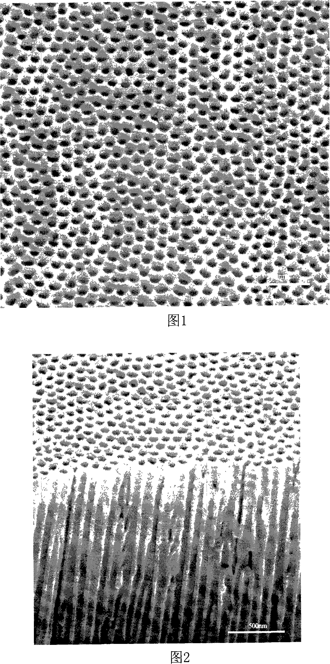
[0029] The obtained aluminum adhered to the silver substrate was placed in a 0.3M / L oxalic acid solution for anodic oxidation. The voltage for oxidation was 40V, the temperature was 5°C (±0.5°C), and the oxidation time was 30 minutes. The prepared aluminum oxide film with nano-holes retains the matrix of the holes and is completely integrated with the silver substrate.
[0030] Use oxalic acid solution with a volume ratio of 5% as the etching solution to etch the aluminum oxide film prepared by the anodic oxidation method. The temperature of the etching solution is 40 degrees Celsius, the stirring rate is 30 rpm, and the etching time is 5 minute.
[0031] Through the above process, a large-area ordered ...
Embodiment 3
[0036] The operation steps as described in Example 1 are performed first to obtain an aluminum oxide film with nano-holes that is completely integrated with the un-oxidized aluminum foil. Then, the unoxidized aluminum foil was removed with a saturated HgCl solution to obtain an aluminum oxide film with nanopores. Copper with a thickness of 20 microns is plated on the aluminum oxide film with nano-holes as a substrate by magnetron sputtering. Use a sulfuric acid solution with a volume ratio of 10% as the etching solution to etch the obtained aluminum oxide film attached to the copper substrate. The temperature of the etching solution is 60 degrees Celsius, and the stirring speed is 50 revolutions per minute. The time is 50 minutes.
[0037]Through the above process, a large-area ordered aluminum oxide nanowire array is prepared.
[0038] The ratio of the length of the nanowires to the root diameter of the nanowires in the nanowire array is 3500nm:62nm=56.45.
[0039] Electro...
PUM
| Property | Measurement | Unit |
|---|---|---|
| length | aaaaa | aaaaa |
| diameter | aaaaa | aaaaa |
| thickness | aaaaa | aaaaa |
Abstract
Description
Claims
Application Information