

Method for preparing column-shape neodymium-doping bismuth titanate ferroelectric thin film used for ferroelectric memory
A ferroelectric memory, neodymium bismuth titanate technology, applied in the direction of ferroelectric carrier recording, can solve the problems of unfavorable anti-fatigue properties and unfavorable compatibility of film capacitors, and achieve the effects of good anti-fatigue properties, large size and low crystallization temperature
- Summary
- Abstract
- Description
- Claims
- Application Information
AI Technical Summary
Problems solved by technology
Method used
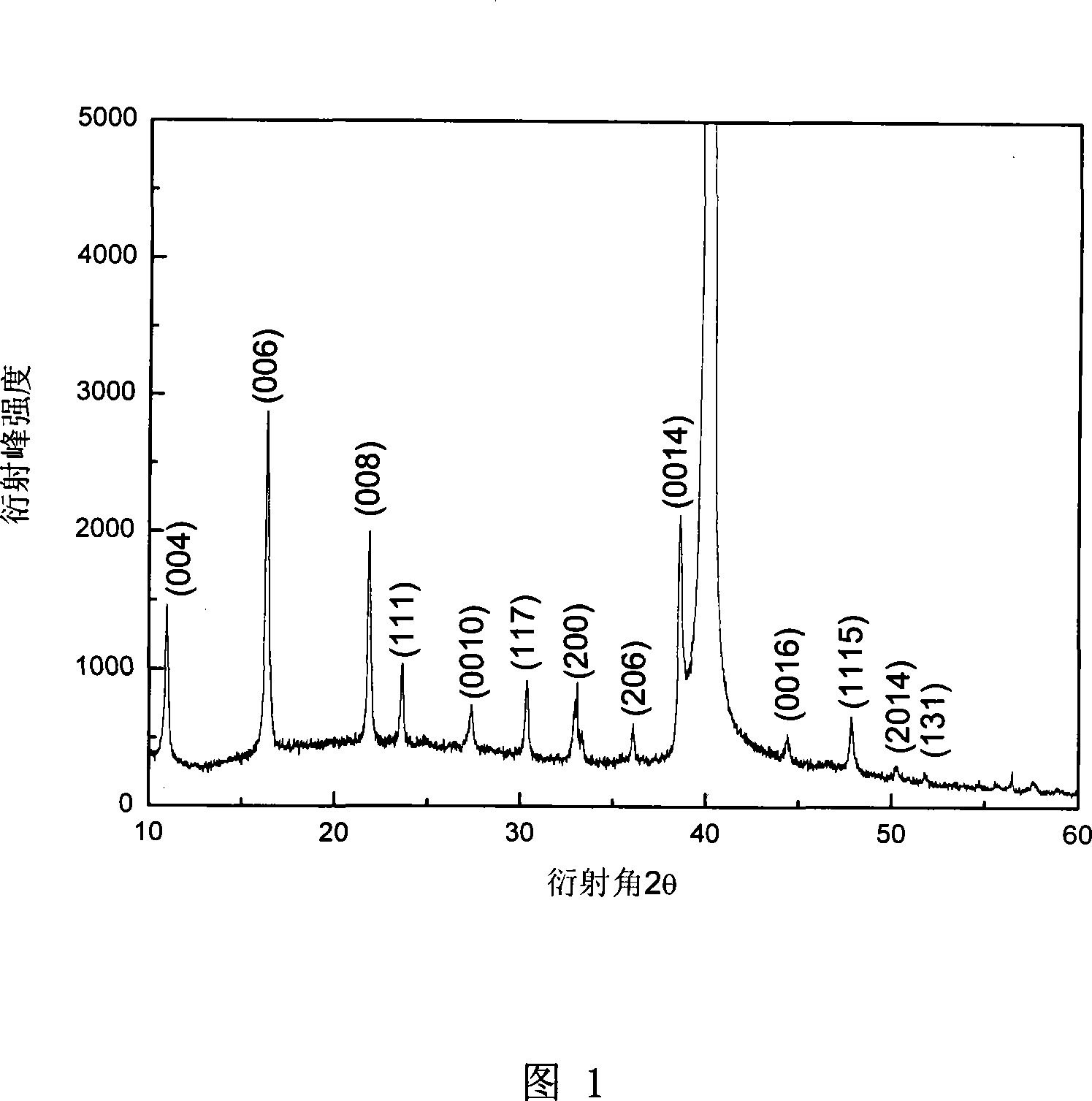
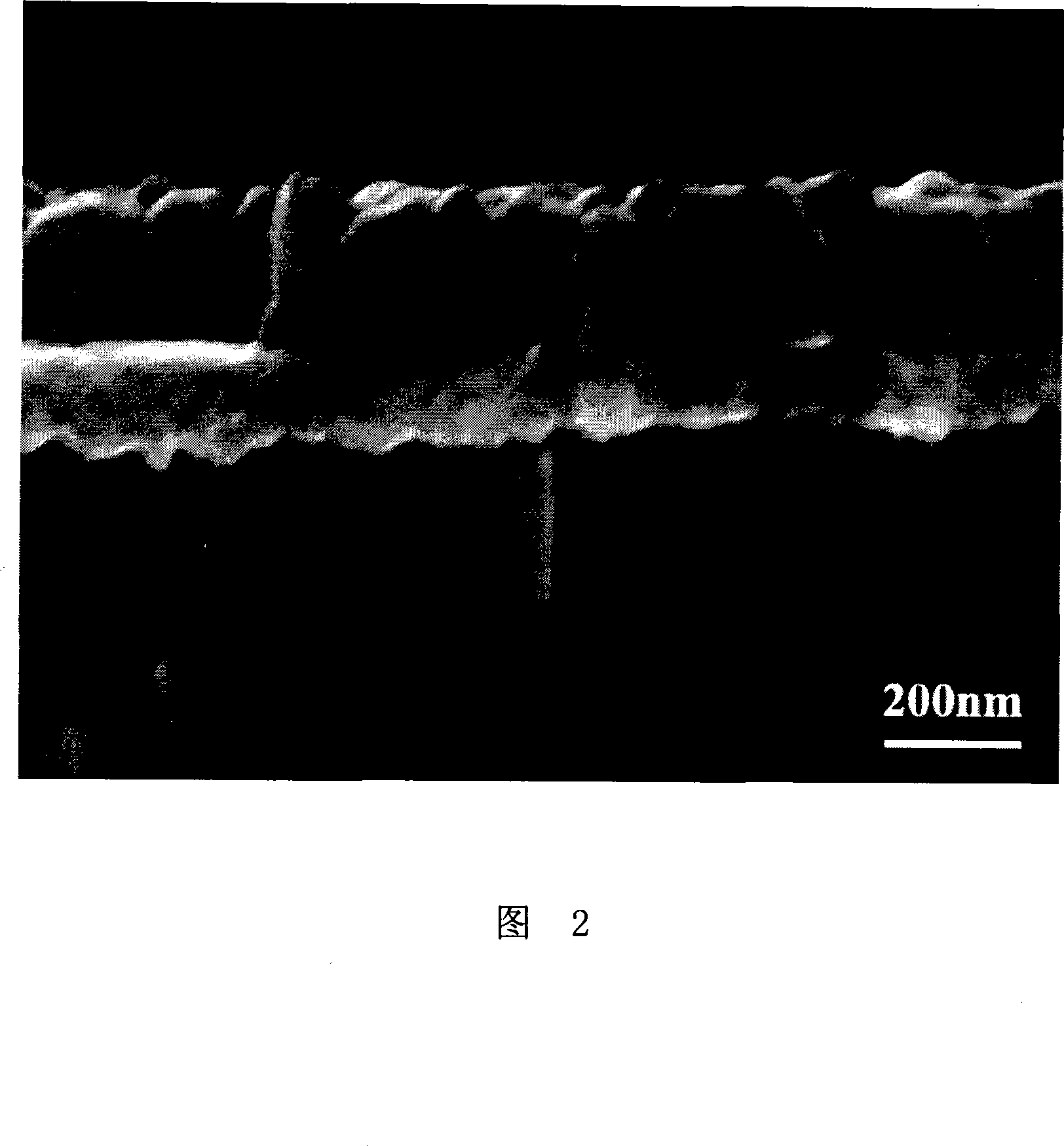
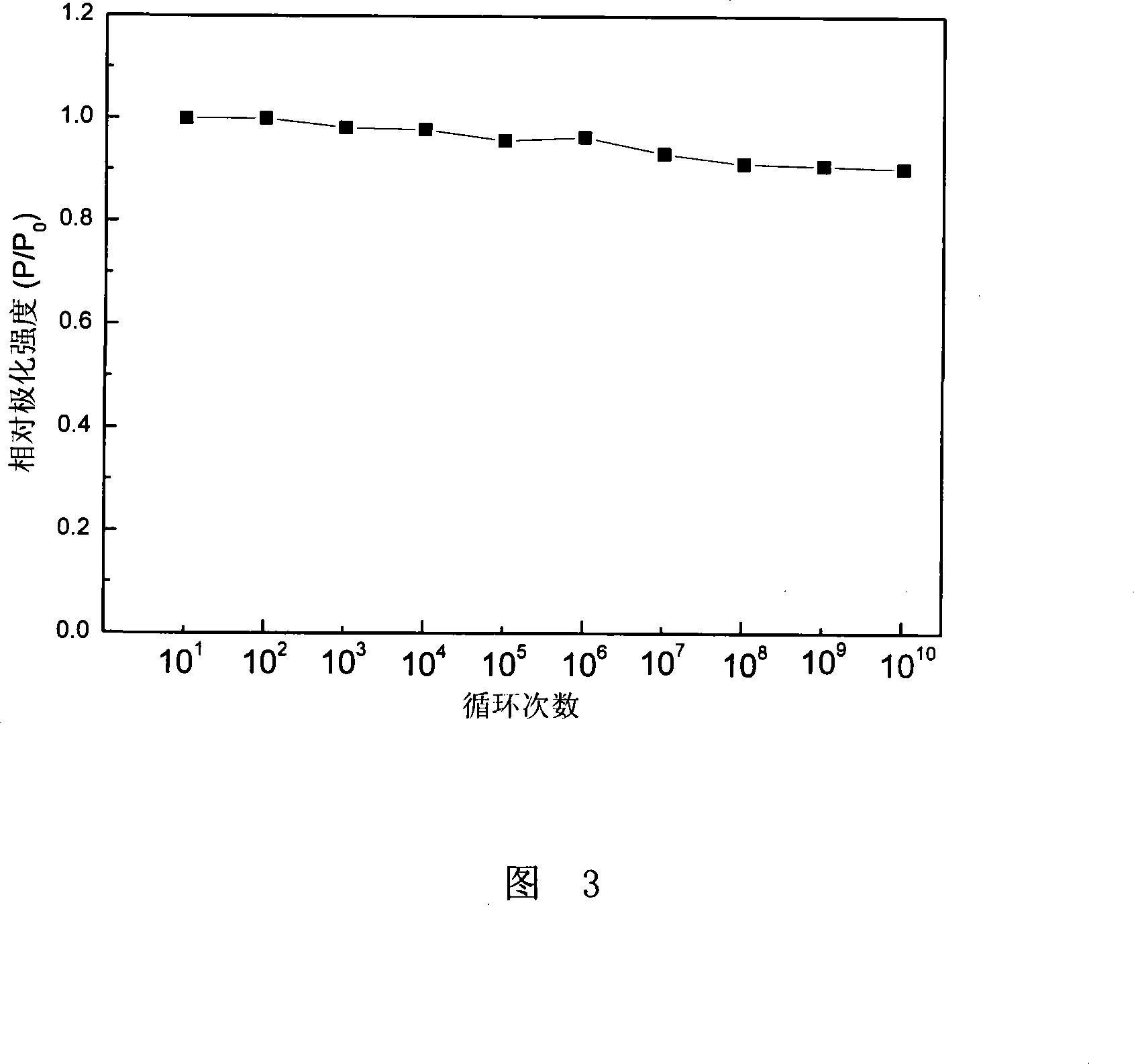
Image

Examples
Embodiment 1
[0031] (1) preparation has Pt as the Si substrate of bottom electrode;
[0032] The specific method is:
[0033] (1.1) surface-treating and cleaning the silicon substrate 1 according to a standard CMOS process;
[0034] (1.2) A silicon dioxide barrier layer 2 with a thickness of 150 nm is formed on the surface of the silicon substrate 1 by a thermal oxidation method;
[0035] (1.3) Prepare a 20nm-thick titanium dioxide bonding layer 3 on the silicon dioxide barrier layer 2 by magnetron sputtering, the process conditions of the magnetron sputtering are: sputtering pressure 1.5Pa, sputtering substrate temperature 200°C , the sputtering atmosphere is O 2 :Ar=1:9;
[0036] (1.4) Prepare the lower electrode metal layer Pt with a thickness of 150nm on the titanium dioxide bonding layer 3 by magnetron sputtering. The shooting atmosphere is Ar gas;
[0037] (2) adopt the following raw materials (its purity is analytically pure 99.9%), use the sol-gel method to prepare the Bi that...
Embodiment 2
[0057] (1) preparation has Pt as the Si substrate of bottom electrode;
[0058] The specific method is:
[0059] (1.1) surface-treating and cleaning the silicon substrate 1 according to a standard CMOS process;
[0060] (1.2) A silicon dioxide barrier layer 2 with a thickness of 150 nm is formed on the surface of the silicon substrate 1 by a thermal oxidation method;
[0061] (1.3) Prepare a 20nm-thick titanium dioxide bonding layer 3 on the silicon dioxide barrier layer 2 by magnetron sputtering, the process conditions of the magnetron sputtering are: sputtering pressure 1.5Pa, sputtering substrate temperature 200°C , the sputtering atmosphere is O 2 :Ar=1:9;
[0062] (1.4) Prepare the lower electrode metal layer Pt with a thickness of 150nm on the titanium dioxide bonding layer 3 by magnetron sputtering. The shooting atmosphere is Ar gas;
[0063] (2) Adopt the following raw materials (its purity is analytically pure 99.9%), use the sol-gel method to prepare the Bi that...
PUM
 Abstract
Description
Claims
Application Information