Semiconductor rectifier device and manufacturing method thereof

A technology of rectifier devices and manufacturing methods, which is applied in semiconductor/solid-state device manufacturing, semiconductor devices, semiconductor/solid-state device components, etc., can solve problems such as unreasonable distribution and large area of ​​vertical MOS tubes, and achieve improved junction characteristics and reduced Parasitic effect, effect of increasing cell density

Inactive Publication Date: 2008-07-23
SUZHOU SILIKRON SEMICON CO LTD
View PDF1 Cites 17 Cited by
  • Summary
  • Abstract
  • Description
  • Claims
  • Application Information

AI Technical Summary

Problems solved by technology

[0015] The present invention provides a semiconductor rectifier device and its manufacturing method, the purpose of which is to solve the problems caused by the large area and unreasonable distribution of the upper source / drain N+ region of the vertical MOS transistor

Method used


Image

  • Semiconductor rectifier device and manufacturing method thereof
  • Semiconductor rectifier device and manufacturing method thereof
  • Semiconductor rectifier device and manufacturing method thereof

Examples


Embodiment 1

[0066] Embodiment 1: a semiconductor rectifier device,

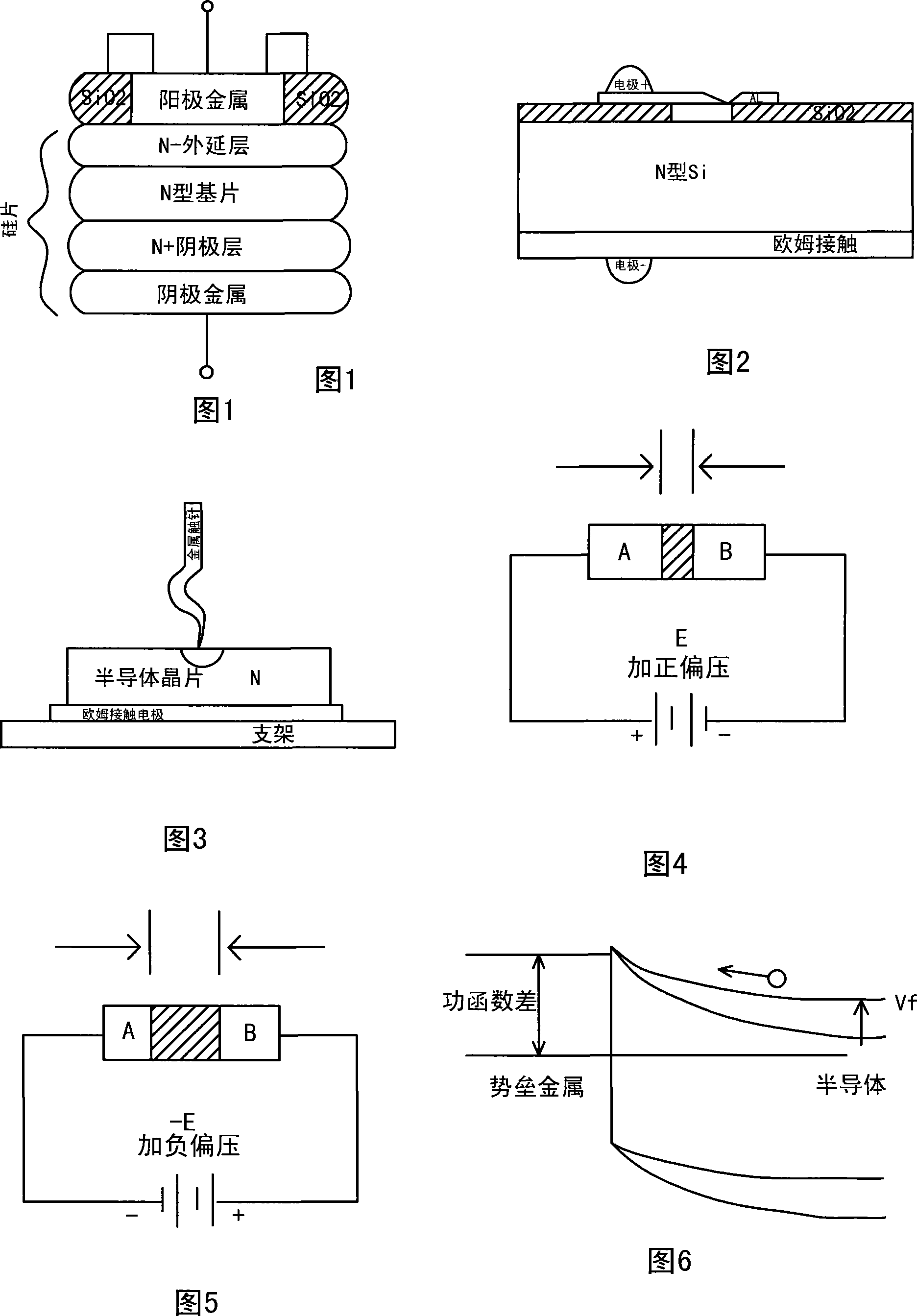
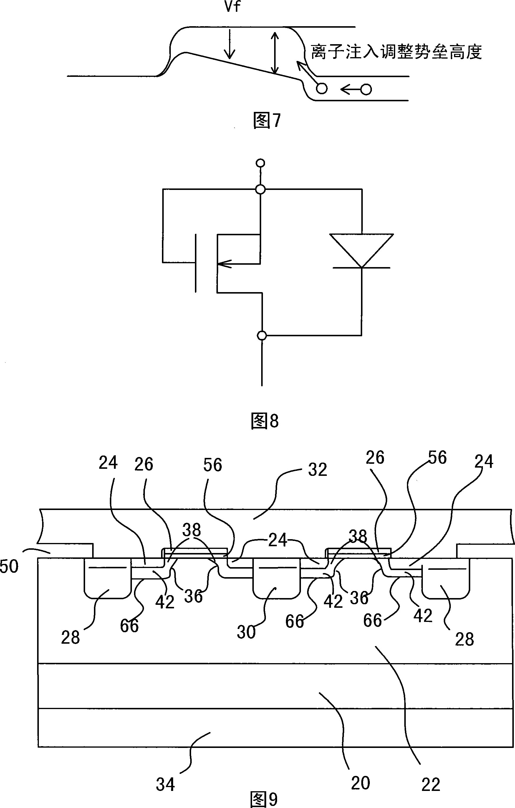
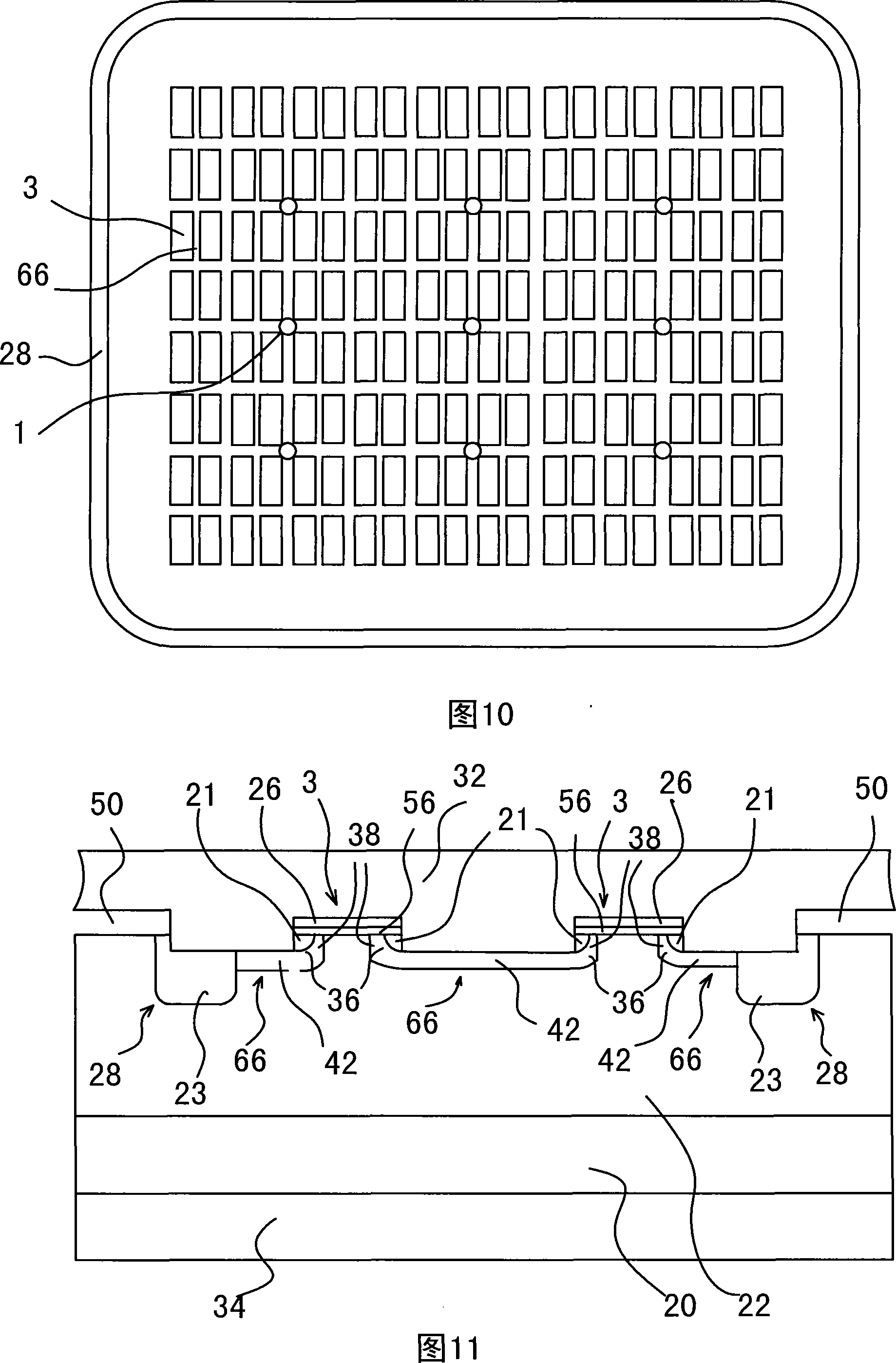
[0067] As shown in FIG. 10 , on a top view plane, the active region of the semiconductor rectifier device is composed of various rectification units arranged and various protection diodes 1 arranged. Each rectifier unit is connected in parallel through upper and lower electrodes to form a whole, wherein each rectifier unit is formed by adjacent combination of PN junction region 66 and vertical semiconductor MOS transistor region 3 . A guard ring 28 is provided around the active area.

[0068] As shown in FIG. 11 , in cross-section, the PN junction region 66 is composed of an upper electrode 32, a second P-diffusion region 42, an N-epitaxial layer 22, an N+ substrate layer 20 and a lower electrode 34 from top to bottom, wherein , the second P-diffusion region 42 and the N-epitaxial layer 22 form the PN junction region.

[0069] As shown in Figure 11, on the cross-section, the vertical semiconductor MOS transistor region...

Embodiment 2

[0073] Embodiment two: a manufacturing method of a semiconductor rectifier device, comprising the following process steps:

[0074] FIG. 12 is a schematic diagram of the manufacturing process of a rectifier device, showing growth of the first silicon oxide layer / photolithography etching of the first P- diffusion region / B+ implantation. Concrete process steps are:

[0075] a) Providing an N-type doped semiconductor silicon wafer having two opposite main surfaces. Wherein, the first main surface refers to the front side of the semiconductor silicon wafer having an N- epitaxial layer, and the second main surface refers to the back side of the semiconductor silicon wafer having an N+ substrate layer.

[0076] b) growing a first silicon oxide layer 25 on the first main surface.

[0077] c) Forming the etching mask pattern of the first P-diffusion region 23 in the first photolithography.

[0078] d) Etching the first silicon oxide layer 25 to open the window of the first P-diffus...


PUM


Abstract

Disclosed are a semiconductor rectifier device and a method for preparation thereof. The device is composed of an equivalent PN junction and a vertical MOS pipe in parallel connection. And an upper source / drain area in the vertical MOS pipe is formed through the following procedures: a, performing N-type ion implantation for an area exposed from a first primary surface of silicon chips after procedures of photo-etching and corroding of a grid electrode, b, performing silicon controlled corrosion for the area exposed from the first primary surface of the silicon chips after implanted by N-type ions, rapidly annealing the N-type ions retained in an area bellow the lateral face of the grid electrode to form the upper source / drain area. The invention resolves the problems brought by the larger surface and unreasonable distribution of the upper source / drain N+ area of the existing vertical MOS pipe through the process of silicon controlled corrosion. For equivalent PN junction areas, a single PN junction is used to replace the original NPN pipe, and thereby the equivalent PN junction areas have fewer parasitic effect of the PN junction. For equivalent vertical MOS pipe areas, residual N-type ions are used to form the upper source / drain area via rapidly annealing, thereby largely reducing effective junction area of the upper source / drain area with smaller reverse leakage current.

Description

technical field [0001] The invention relates to a power semiconductor MOS device and a manufacturing method thereof, in particular to a semiconductor rectifying device and a manufacturing method thereof. This MOS device retains the advantages of Schottky barrier rectifier diodes, and at the same time has the characteristics of fast forward conduction, low reverse leakage, and the conduction voltage Vf can be adjusted by ion implantation dose. In addition, the device does not require barrier precious metals, and can be manufactured by standard CMOS silicon technology, so the reliability of the device is high and the cost can be greatly reduced. Background technique [0002] Schottky barrier rectifier diodes use noble metals (such as gold, silver, platinum, titanium, nickel, molybdenum, etc.) A semiconductor device made of potential barriers. Its working principle is: there are a large number of electrons in N-type semiconductors, and there are only a small amount of free el...

Claims


Application Information

Patent Timeline
Patent Type & Authority Applications(China)
IPC IPC(8): H01L21/336H01L27/06H01L23/522H01L29/78H01L29/08H01L21/822
Inventor 朱袁正周名辉钱叶华
Owner SUZHOU SILIKRON SEMICON CO LTD
Why Eureka
Try Eureka