Back irradiation arsenic indium table face line array or face array detector chip and its making technology

A detector chip, InGaAs technology, applied in sustainable manufacturing/processing, semiconductor devices, final product manufacturing, etc., can solve the problem of device responsivity and quantum efficiency reduction, limit the performance of InGaAs detectors, and limit the uniformity of devices Improve the performance and other issues to achieve the effect of reducing the surface charge density and interface state density, improving the responsivity and detection rate, and reducing the dark current

Active Publication Date: 2008-08-13
SHANGHAI INST OF TECHNICAL PHYSICS - CHINESE ACAD OF SCI
View PDF1 Cites 12 Cited by
  • Summary
  • Abstract
  • Description
  • Claims
  • Application Information

AI Technical Summary

Problems solved by technology

InGaAs back-illuminated long-line array and area array detectors mostly use planar junction technology, but planar junction has some unavoidable disadvantages: complex diffusion process, enlarged photosensitive surface and zinc (Zn) diffusion will be in the indium phosphide (InP) layer. A large number of defects are caused, which limit the improvement of the performance of InGaAs detectors
The mesa-type indium gallium arsenide detector is to etch the p-type indium phosphide/indium gallium arsenide (p-InP/InGaAs) in the epitaxial material into a mesa. The advantage of this structure is that the process is relatively simple, and the disadvantage is that the side and surface Exposure will introduce a large number of interface states, which will limit the improvement of the uniformity of long

Method used


Image

  • Back irradiation arsenic indium table face line array or face array detector chip and its making technology
  • Back irradiation arsenic indium table face line array or face array detector chip and its making technology
  • Back irradiation arsenic indium table face line array or face array detector chip and its making technology

Examples


Embodiment Construction

[0023] The specific implementation method of the present invention will be described in detail below in conjunction with the accompanying drawings and embodiments.

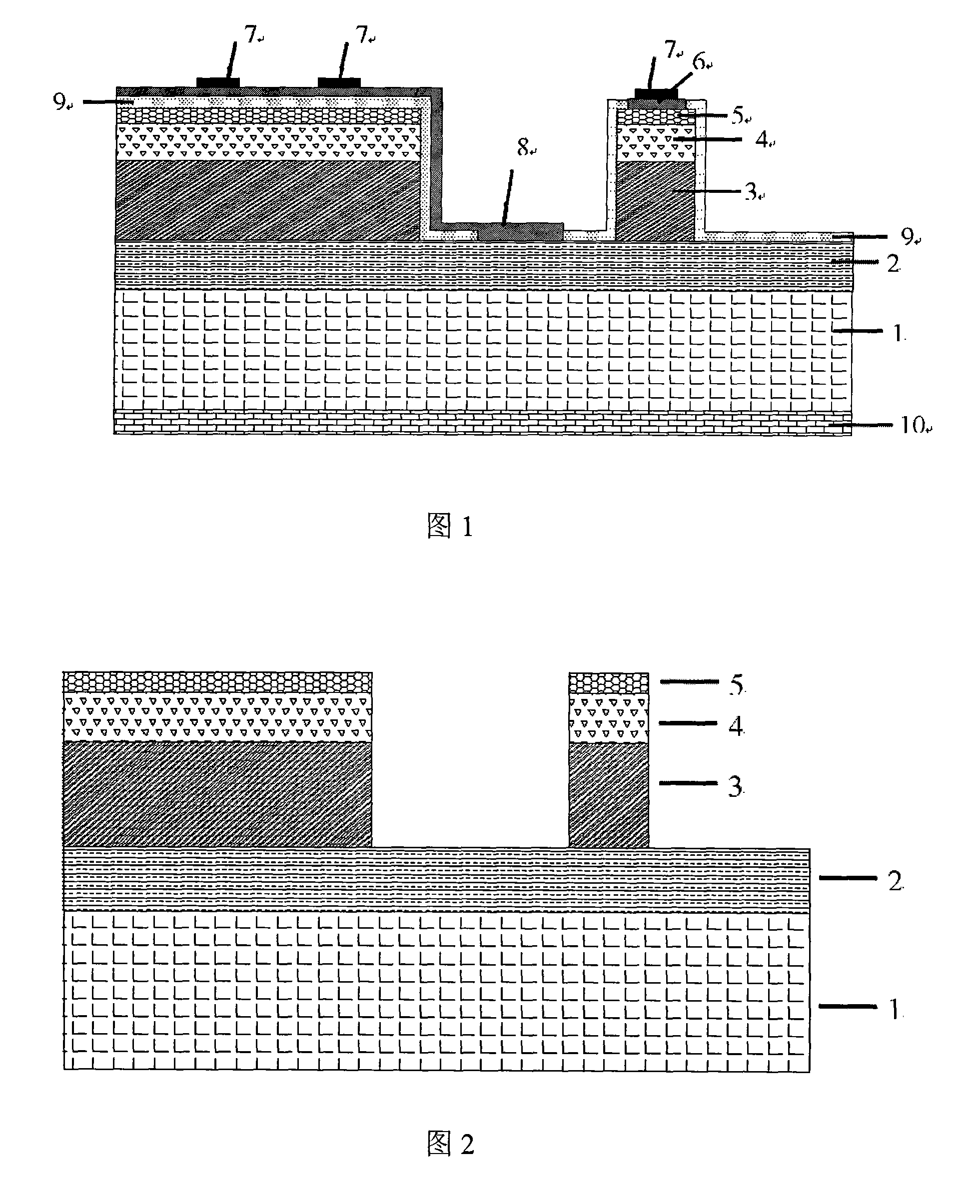
[0024] As shown in Figure 1, the epitaxial wafer used in the detector of this embodiment is an N-type InP layer 2 with a thickness of 1 μm grown sequentially on a semi-insulating InP substrate 1 with a thickness of 350 μm by MBE technology, and the carrier concentration is greater than 2 ×10 18 cm -3 ; In thickness of 1.1 μm to 1.5 μm 0.53 Ga 0.47 As absorption layer 3, the carrier concentration is 5×10 16 cm -3 ; P-type InP cap layer 4 with a thickness of 0.5 μm, the carrier concentration is greater than 2×10 18 cm -3 ; The uppermost layer grows a p-InGaAs layer 5 with a thickness of 20nm and a carrier concentration of 2×10 18 cm -3 . On the epitaxial wafer, the linear p-InGaAs / p-InP / i-InGaAs micro-mesas are formed by etching, and there is a Ti / Pt / Au electrode region 6 in ohmic contact with p-InGaAs on t...


PUM

PropertyMeasurementUnit
Thicknessaaaaaaaaaa

Abstract

The present invention discloses a back-irradiating indium gallium arsenic micro-table-board detector chip and the preparation technique thereof, the preparation technique comprises etching on the p-InGaAs/p-InP/i-InGaAs/n-InP epitaxial slice to form the p-InGaAs/p-InP/i-InGaAs micro-table-board, the thickness of the InGaAs absorption layer is designed to 1.1um to 1.5um, the doping concentration is 3-5*10<16>cm<-3>, the +SiNx passivating film is vulcanized and the annealing technique is leaded in, and the purposes of effectively reducing the combination of surface and side surface, reducing the density of interfacial state and increasing the detectivity and homogeneity of the device, the leading-out area of the p type electrode is grown with a layer of p-InGaAs electrode transition layer, the contact between the Ti/Pt/Au electrode grown by the evaporation of the electron beam and the p-InGaAs is excellent ohm contact, the small contact resistance increases the capability of the detector, at the same time the back-irradiating mode is adopted and the incident light will not be absorbed by the p-InGaAs of the p type electrode leading-out layer, the response ratio of the device is facilitated to be increased and the back low-temperature deposition ZnS reflection reducting coating can further increase the repose ratio and quantum efficiency of the device.

Description

technical field [0001] The invention relates to an infrared detection device and its manufacturing technology, specifically a back-illuminated indium gallium arsenide (InGaAs) micro-mesa line or area array detector chip and its preparation process, which is suitable for making high-uniformity long line or area arrays InGaAs micro-mesa focal plane detector. Background technique [0002] InGaAs short-wave infrared detectors can work at room temperature, and their performance is better than short-wave antimony-cadmium mercury (HgCdTe) detectors, so they have broad application prospects in military and civilian fields. InGaAs back-illuminated long-line array and area array detectors mostly use planar junction technology, but planar junction has some unavoidable disadvantages: complex diffusion process, enlarged photosensitive surface and zinc (Zn) diffusion will be in the indium phosphide (InP) layer. A large number of defects are caused, which limit the improvement of the perf...

Claims


Application Information

Patent Timeline
IPC IPC(8): H01L31/105H01L31/18
CPCY02P70/50
Inventor 唐恒敬张可锋吴小利朱慧宁锦华李淘汪洋李雪李永富龚海梅
Owner SHANGHAI INST OF TECHNICAL PHYSICS - CHINESE ACAD OF SCI
Why Eureka
Try Eureka