Laser etching and trench digging method of semiconductor chip

A laser etching and semiconductor technology, applied in semiconductor/solid-state device manufacturing, laser welding equipment, electrical components, etc., can solve the problems of deposition on the side of the engraved pattern, pattern deformation, poor selectivity, etc., and achieve good consistency , small thermal effect and low cost

Inactive Publication Date: 2008-08-20
SUZHOU GOODARK ELECTRONICS CO LTD
View PDF0 Cites 20 Cited by
  • Summary
  • Abstract
  • Description
  • Claims
  • Application Information

AI Technical Summary

Problems solved by technology

However, in dry etching, the residual oxygen will etch the photoresist, and the temperature in the reaction chamber can be as high as 200°C. A certain high temperature can bake the photoresist to a state that is difficult to remove from the wafer. The temperature effect will also deform the pattern due to the flow t

Method used


Image

  • Laser etching and trench digging method of semiconductor chip
  • Laser etching and trench digging method of semiconductor chip

Examples


Embodiment

[0038] Embodiment: A semiconductor wafer laser etching trenching method, which consists of two parts: laser etching to form a trench and post-processing.

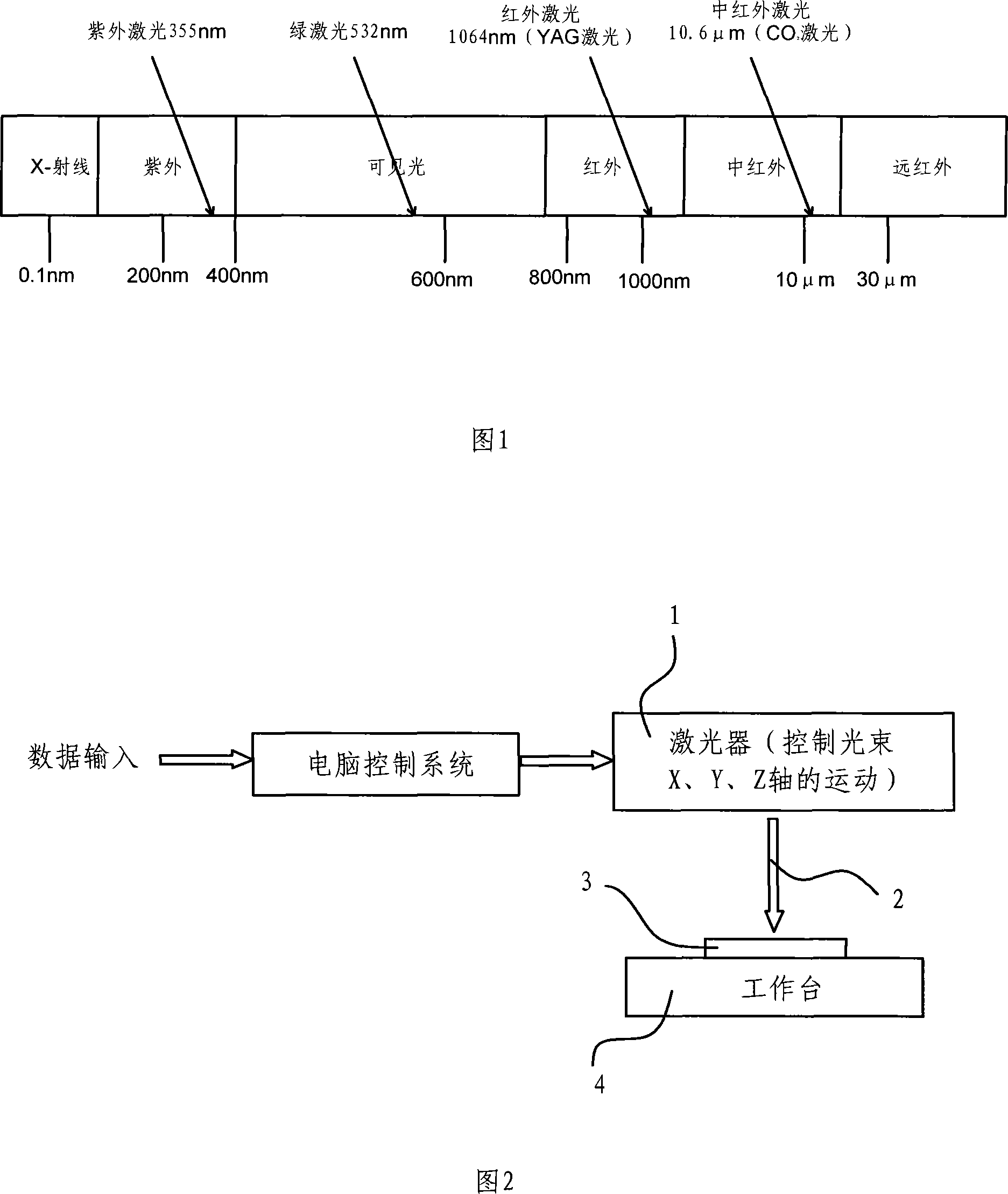
[0039] As shown in Figure 2, laser etching forms the groove by fixing the semiconductor wafer 3 on the workbench 4 through the clamp, and utilizing the laser beam 2 emitted by the laser 1 to radiate the surface of the semiconductor wafer 3 vertically, along with the laser beam 1 and the semiconductor wafer 3 On the moving path, the laser beam 2 etches the material on the surface layer of the radiation area by melting and evaporating, thereby forming grooves on the surface of the semiconductor wafer 3 .

[0040] The laser beam 2 is an ultraviolet laser with a wavelength of 200-400 nanometers, as shown in Figure 1, this laser is a cold laser light source with a small thermal effect area, so it will not damage the semiconductor lattice outside the radiation area. In addition, the operating frequency of the laser beam 2 is sele...


PUM

PropertyMeasurementUnit
Wavelengthaaaaaaaaaa

Abstract

The invention relates to a method for laser etching trenching of a semiconductor wafer, characterized in: a semiconductor wafer surface is vertically radiated by a laser beam, with the relative movement between the laser beam and the semiconductor wafer, the laser beam etches the material on the surface of the radiation area by way of melting and evaporating, thus to form a trench on the semiconductor wafer surface; the laser beam is ultraviolet laser, the wavelength is 200 to 400nm, the frequency is 30 to 50 KHz, the single pulse energy is 100 to 200 mJ. The invention relates to the field of semiconductor manufacture technology, which is environment-friendly and efficient, overcomes the drawbacks of past method that trenches by wet etching or dry etching, improves the accuracy, stability and uniformity, lowers the cost, and enriches the processing technology for surface etching trenching of semiconductor wafer.

Description

technical field [0001] The invention relates to semiconductor manufacturing technology, in particular to a method for using laser etching to open grooves on the surface of a semiconductor wafer. The method is not only environmentally friendly and efficient, but also simplifies the processing technology of traditional semiconductor surface ditching, improves the ditching accuracy, and reduces the cost. Background technique [0002] In the semiconductor chip processing technology, several main steps such as oxidation, deposition, photolithography, etching, ion implantation and metallization are widely used, and trenching on the semiconductor wafer is an indispensable process method after pattern exposure. [0003] In the prior art, the so-called trenching is to use the geometric patterns on the mask (Mask) to transfer the patterns to the photosensitive film (photoresist) covered on the semiconductor wafer through photochemical reaction. These patterns can define various aspect...

Claims


Application Information

Patent Timeline
IPC IPC(8): H01L21/302B23K26/36B23K26/362
Inventor 吴念博
Owner SUZHOU GOODARK ELECTRONICS CO LTD
Why Eureka
Try Eureka