Coaxial double-pipe titanium dioxide nano-pipe array thin film and preparation method thereof
A technology of nanotube array and titanium dioxide, which is applied in the direction of titanium dioxide, chemical instruments and methods, titanium oxide/hydroxide, etc., can solve the problems that have not yet been reported on the nanotube array structure, and achieve excellent photocatalytic performance, high biological activity, Significant semiconductor performance effects
- Summary
- Abstract
- Description
- Claims
- Application Information
AI Technical Summary
Problems solved by technology
Method used
Image
Examples
Embodiment 1
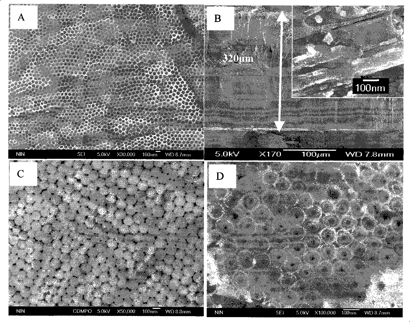
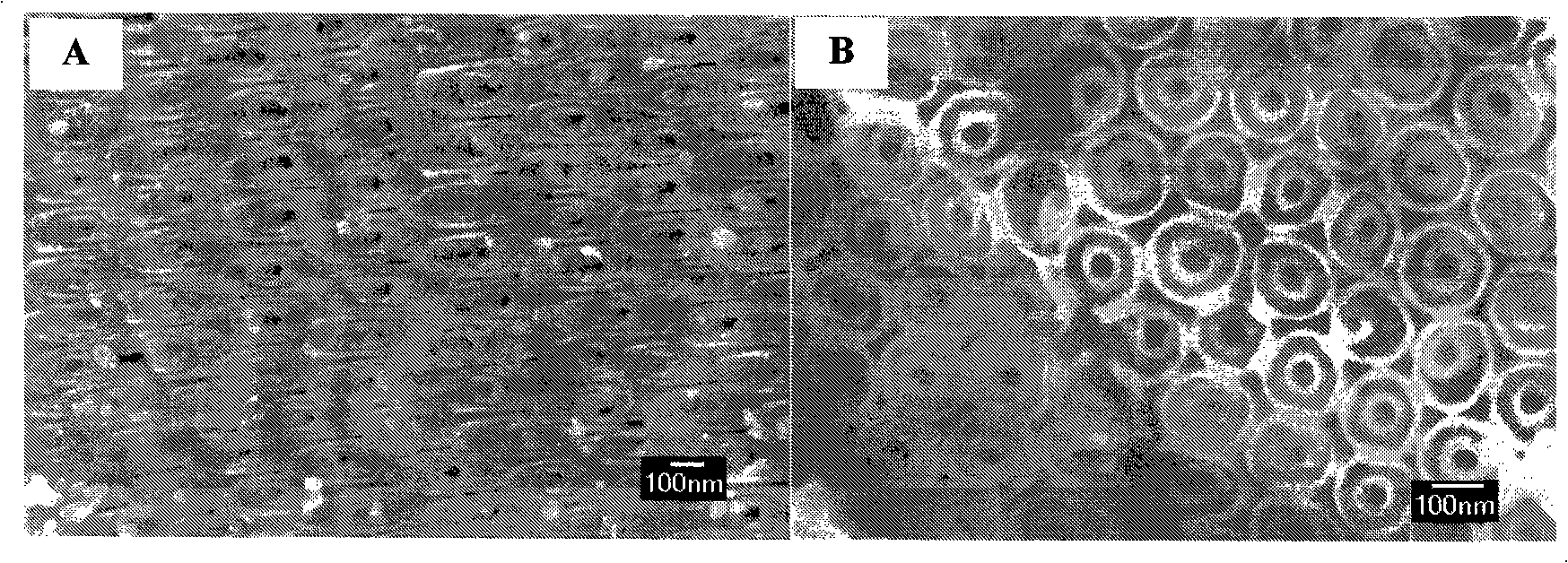
[0024] Mechanically process the TLM sheet into a sheet of 500mm×100mm×1mm, polish it brightly with 150#, 600#, 1000# sandpaper, then ultrasonically degrease in ethanol and acetone, clean with deionized water, 70℃~80℃ Dry in a hot air oven; applied voltage 50V, in 0.25wt%NH 4 F, 1.0wt%H 2 O in ethylene glycol solution, anodized for 4320min to obtain nanotube arrays. The nanotube array was washed several times with deionized water, placed in a drying oven, and dried at 70° C. to 80° C. for 1 hour. Then, the obtained nanotube array thin film. The obtained nanotube array film was removed from the substrate, fixed on a hollow PVC plate, and then the PVC was placed on the mouth of a plastic bottle filled with saturated HF acid, so that the bottom surface of the nanotube array was in an HF acid atmosphere. The gas removes the barrier layer at the bottom of the nanotube array film, and the FE-SEM image of the nanotube array prepared by this process, as shown in figure 1 shown.
...
Embodiment 2
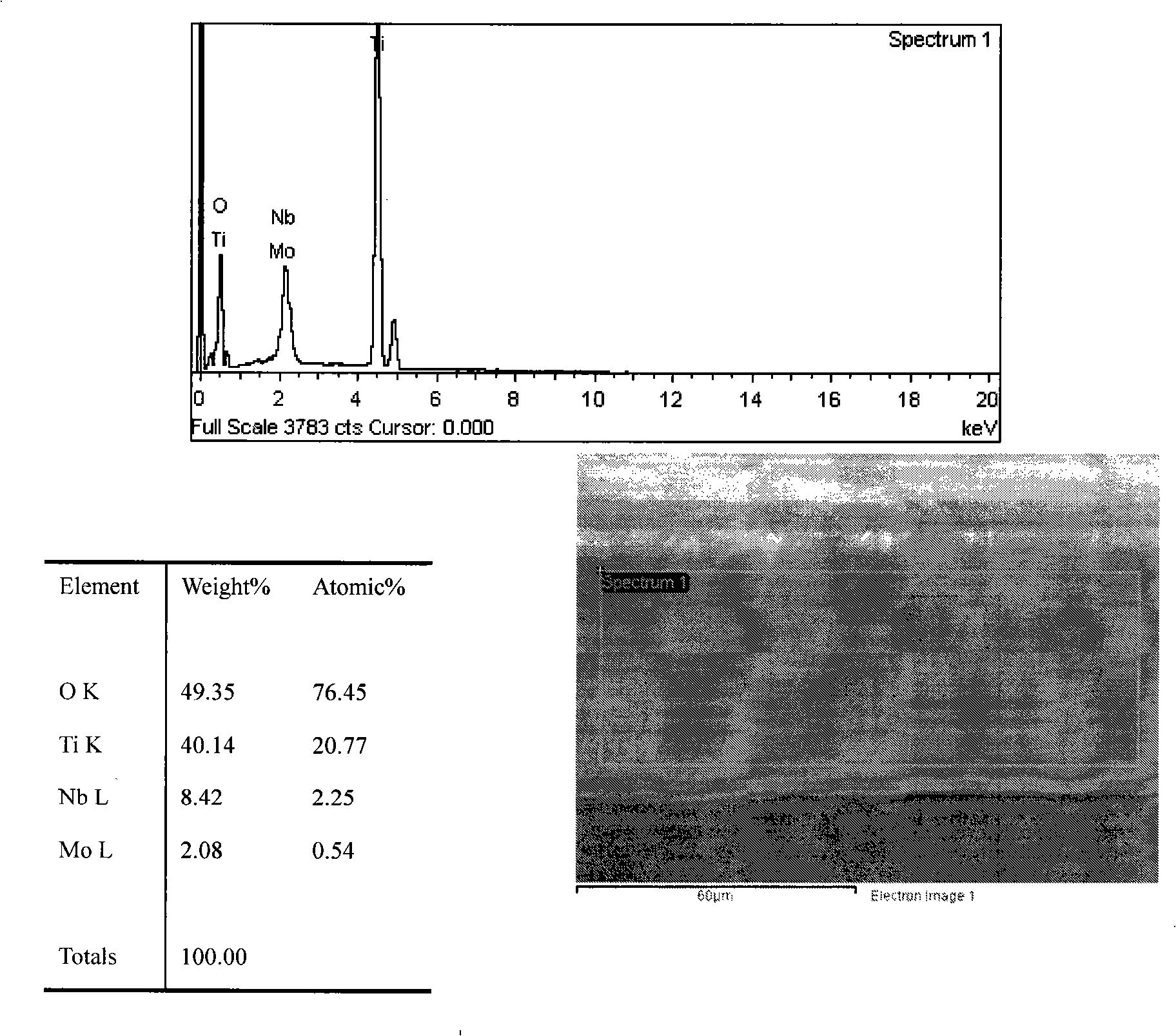
[0027]Mechanically process the TLM sheet into a sheet of 300mm×20mm×1mm, polish it brightly with 150#, 600#, 1000# sandpaper, then ultrasonically degrease in ethanol and acetone, clean with deionized water, 70℃~80℃ Dry in a hot air oven; applied voltage 40V, in 0.25wt% NH 4 F, 1.0wt%H 2 Coaxial TiO doped with Nb and other elements prepared by anodizing in ethylene glycol solution of O for 480 min 2 array of nanotubes. The nanotube array was washed several times with deionized water, placed in a drying oven, and dried at 70° C. to 80° C. for 1 hour. The EDS energy spectrum of the nanotube array film prepared by this process is as follows image 3 shown.
[0028] The coaxial TiO doped with elements such as Nb prepared on the surface of the TLM alloy in this example 2 The nanotube array film can improve the growth and attachment ability of osteoblasts on the surface of TLM alloy. Compared with Ti alloy surface nanotube arrays, coaxial TiO 2 Osteoblasts grow more efficientl...
Embodiment 3
[0030] Mechanically process the TLM sheet into a sheet of 300mm×20mm×1mm, polish it brightly with 150#, 600#, 1000# sandpaper, then ultrasonically degrease in ethanol and acetone, clean with deionized water, 70℃~80℃ Dry in a hot air oven; applied voltage 50V, in 0.25wt%NH 4 F, 1.0wt%H 2 Coaxial nanotube array film prepared by anodizing in ethylene glycol solution of O for 4320min. The nanotube array thin film was washed with deionized water several times, placed in a drying oven, and dried at 70° C. to 80° C. for 1 hour. The sample was annealed in an oxygen atmosphere in a muffle furnace, the heating and cooling rate was controlled at 1 °C / min, the constant temperature point was 500 °C, and the temperature was kept for 120 min. The X-ray diffraction pattern of the nanotube array prepared by this process is as follows: Figure 4 shown.
PUM
| Property | Measurement | Unit |
|---|---|---|
| Thickness | aaaaa | aaaaa |
Abstract
Description
Claims
Application Information


