Si-Si bonding isolator upper silicon high-temperature pressure sensor chip and manufacture method

A technology of a pressure sensor and a manufacturing method, which is applied in the fields of semiconductor/solid-state device parts, piezoelectric/electrostrictive/magnetostrictive devices, and the measurement of the property force of piezoresistive materials, etc., can solve the problem of process stability. High, it is difficult to ensure the uniformity of the stress film, etc., to achieve the effect of ensuring long-term stability, suitable for mass production, and small residual stress

Inactive Publication Date: 2008-09-17
SHANGHAI INST OF MICROSYSTEM & INFORMATION TECH CHINESE ACAD OF SCI
View PDF0 Cites 43 Cited by
  • Summary
  • Abstract
  • Description
  • Claims
  • Application Information

AI Technical Summary

Problems solved by technology

[0003] Ordinary SOI high temperature pressure sensors (such as Q.Wang et al. published in Sensors and Actuators A120 (2005) page 468 on Fabrication and temperature coefficient compensation technology of low cost high temperature pressure sensor article) take a long time an

Method used


Image

  • Si-Si bonding isolator upper silicon high-temperature pressure sensor chip and manufacture method
  • Si-Si bonding isolator upper silicon high-temperature pressure sensor chip and manufacture method
  • Si-Si bonding isolator upper silicon high-temperature pressure sensor chip and manufacture method

Examples


Embodiment Construction

[0018] The following examples will help to understand the present invention, but do not limit the content of the present invention. The manufacturing method of silicon-on-insulator high-temperature pressure sensor chip suitable for silicon-silicon bonding in the range of 1MPa:

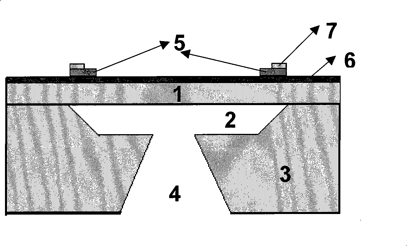
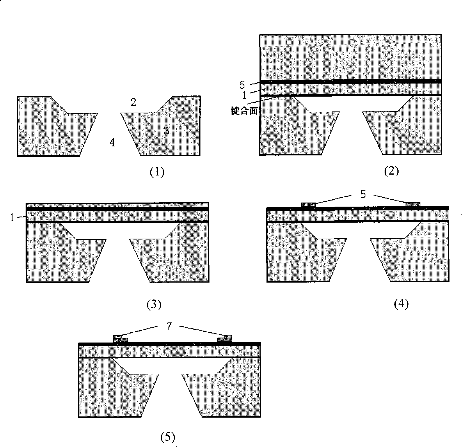
[0019] Using 4-inch 450μm N-type (100) double-polished single-crystal silicon wafers, the resistivity is 1-10ohm.cm, and 4-inch P-type double-polished SOI wafers, the thickness of the top silicon layer and the buried layer are 60 microns and 1 micron respectively , the top silicon resistivity 1-10ohm.cm.

[0020] 1. Clean the silicon wafer and then oxidize it. Use front and back photolithography to align, and use the oxide layer as a mask to etch shallow grooves and air guide holes in KOH solution, corresponding to image 3 (1);

[0021] 2. SOI wafers and silicon wafers are bonded on the shallow groove surface. Use 400°C vacuum in the bonding machine, pressurize 2bar for 20 minutes, and then dry oxygen...


PUM

PropertyMeasurementUnit
Thicknessaaaaaaaaaa

Abstract

The invention relates to a high-temperature press sensor of silicon-silicon-bonded-based silicon on an insulator (SOI) and a producing method, belonging to the field of sensor chip, characterized in that a shallow slot and a gas vent on a support silicon substrate are all formed through anisotropic etch; suitable depth of the shallow slot can be obtained by controlling etching time so as to accomplish over-voltage protection for the device; the support silicon substrate is bonded with an inverted SOI chip; a piezoresistor is produced on the top layer of silicon after reducing and polishing the back of the SOI chip. The device can operate normally at high temperature using SOI buried oxide layer for isolation of sensitive component and elastic component.

Description

technical field [0001] The invention relates to a silicon-on-insulator silicon-on-insulator (SOI) high-temperature pressure sensor chip and a manufacturing method thereof, which belong to the field of sensor chips. Background technique [0002] As the most commercially successful MEMS device, silicon-based pressure sensors have been widely used and technologically advanced in the fields of petroleum, aerospace, medical equipment, and automotive electronics in the past few decades. However, because the traditional bulk silicon pressure sensor uses a pn junction as an electrical isolation means, it will eventually fail due to the increase of the reverse leakage current in an environment above 125 ° C (Diem et al. published on pages 8 of Sensors and Actuators A 46-47 (1995) SOI 'SIMOX' from bulk to surface micromachining, a new age for silicon sensors and actuators. A paper). The use of SOI materials can play a significant role in improving the high temperature performance of ...

Claims


Application Information

Patent Timeline
IPC IPC(8): G01L1/18B81B7/02B81C1/00
Inventor 武爱民陈静王曦魏星张波
Owner SHANGHAI INST OF MICROSYSTEM & INFORMATION TECH CHINESE ACAD OF SCI
Why Eureka
Try Eureka