Planar MOSFET integrated with schottky diode and its layout method

一种栅极、顶表面的技术,应用在二极管、半导体器件、电气元件等方向,能够解决易发生击穿曲率半径、高成本等问题

Active Publication Date: 2009-04-08
ALPHA & OMEGA SEMICON INC
View PDF3 Cites 15 Cited by
  • Summary
  • Abstract
  • Description
  • Claims
  • Application Information

AI Technical Summary

Problems solved by technology

However, the high barrier height metal required to achieve a suitably low leakage current in the off state has the disadvantage of meeting the Schottky ohmic contact and the source-body ohmic contact at the same time. Depositing high barrier height metals and lower barrier height metals incurs higher cost
[0006] In addition, in Figure 1A , Figure 1B and figure 2 The device structure shown in is still subject to the Figure 1C and Figure 1D The bottom corner of the P+ pocket region shown in is easily limited by the breakdown characteristics. The breakdown is easy to occur at the bottom corner of the body-type doped (P+ pocket) region because of the vicinity of the bottom corner of the P+ pocket region. Due to the small radius of curvature of the PN junction

Method used


Image

  • Planar MOSFET integrated with schottky diode and its layout method
  • Planar MOSFET integrated with schottky diode and its layout method
  • Planar MOSFET integrated with schottky diode and its layout method

Examples


Embodiment Construction

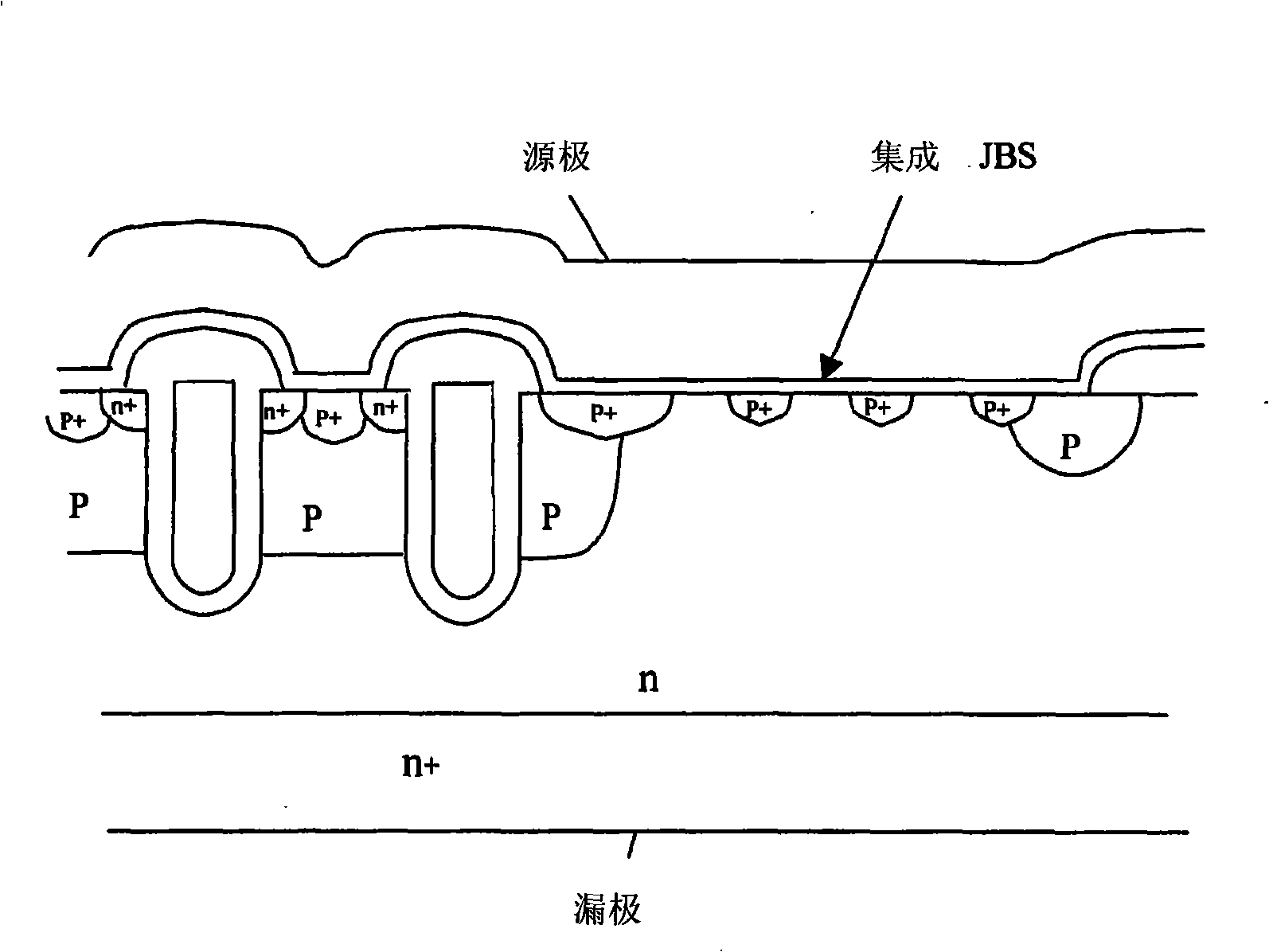
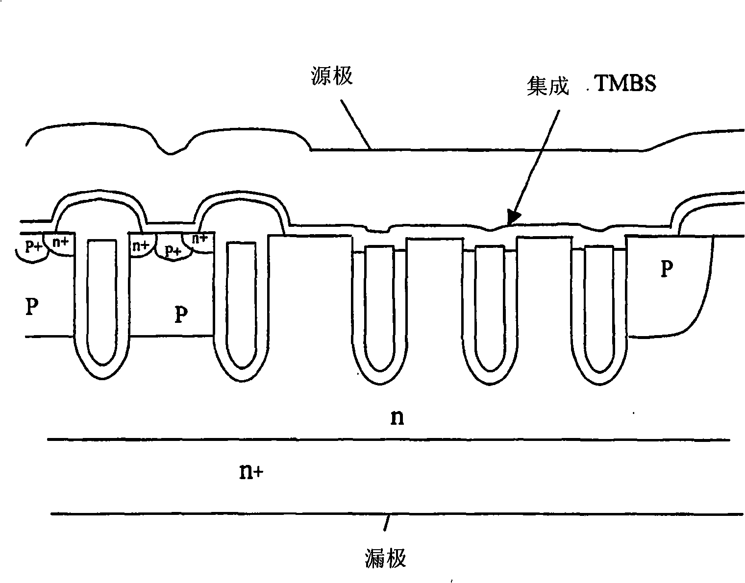
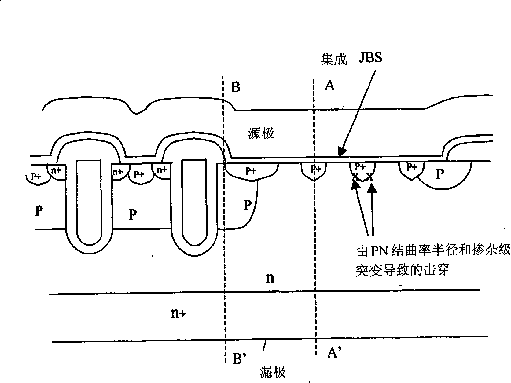
[0038] Such as Figure 3A and Figure 3B Shown is a schematic side cross-sectional view of the JBS region that provides the MOSFET device modification function, Figure 3A Blank implantation of body-type shallow dopant ions is shown. For N-channel MOSFET devices, the doping concentration is 5×10 11 / cm 2 ~5×10 12 / cm 2 The boron ions are implanted into the epitaxial layer, and the implantation energy is 40-500Kev, preferably 80-300Kev. The blank implantation of body-type ions compensates and reduces the doping concentration of a part of the epitaxial layer, thereby increasing the breakdown voltage of the epitaxial layer. exist Figure 3B , using higher diffusion temperatures (ranging from 1000°C to 1150°C for 1 to 3 hours) to diffuse the body-type dopant to a shallower depth than the MOSFET body region formed in subsequent steps, the implanted The doping ions of the body region type compensate the doping of the epitaxial layer, and generate N-regions in the epitaxial l...


PUM


Abstract

A planar MOSFET integrated with Schottky diodes manufactured without additional masks and layout method. A semiconductor power device supported on a semiconductor substrate of a first conductivity type with a bottom layer functioning as a bottom electrode and an epitaxial layer overlying the bottom layer with a same conductivity type as the bottom layer. The semiconductor power device includes a plurality of FET cells and each cell further includes a body region of a second conductivity type extending from a top surface into the epitaxial layer. The body region encompasses a heavy body dopant region of second conductivity type. An insulated gate is disposed on the top surface of the epitaxial layer, overlapping a first portion of the body region. A barrier control layer is disposed on the top surface of the epitaxial layer next to the body region away from the insulated gate. A conductive layer overlies the top surface of the epitaxial layer covering a second portion of the body region and the heavy body dopant region extending over the barrier control layer forming a Schottky junction diode.

Description

technical field [0001] The present invention relates to a semiconductor power device, in particular to an improved and novel manufacturing process and device structure for integrating a silicon carbide mixed Schottky tube onto a planar MOSFET (Metal Oxide Semiconductor Field Effect Transistor). No additional masks are required to improve high frequency power conversion, H-bridge and synchronous rectification applications. Improved body diode recovery results in lower losses and lower voltage oscillations in the power circuit without compromising the layout of the integrated MOSFET Schottky device. Background technique [0002] In order to reduce power loss in semiconductor power devices while increasing their switching speed, further reductions in on-resistance and gate capacitance are desired. Integrals in which Schottky diodes are disposed over semiconductor power devices such as Metal Oxide Silicon Field Effect Transistors (MOSFETs) have been used. In addition to the de...

Claims


Application Information

Patent Timeline
Patent Type & Authority Applications(China)
IPC IPC(8): H01L27/06H01L21/822
CPCH01L29/0692H01L29/7813H01L29/456H01L29/1095H01L29/0619H01L29/8725H01L29/7811H01L29/7806H01L29/0696H01L29/872H01L29/66734H01L29/4236H01L29/47H01L29/0878
Inventor 安荷·叭剌
Owner ALPHA & OMEGA SEMICON INC
Why Eureka
Try Eureka