Three-dimensional quantum well NMOS integrated component and preparation method thereof

A technology of integrated devices and quantum wells, applied in semiconductor/solid-state device manufacturing, electric solid-state devices, semiconductor devices, etc., can solve the problem of low speed, reduce carrier scattering, enhance carrier transport capacity, The effect of improving electrical performance

Inactive Publication Date: 2010-08-25
XIDIAN UNIV
View PDF0 Cites 0 Cited by
  • Summary
  • Abstract
  • Description
  • Claims
  • Application Information

AI Technical Summary

Problems solved by technology

[0012] The purpose of the present invention is to overcome the low speed of existing three-dimensional integrated devices, and provide a three-dimensional quantum well NMOS integrated device and its manufacturing method to improve the performance of integrated circuits

Method used


Image

  • Three-dimensional quantum well NMOS integrated component and preparation method thereof
  • Three-dimensional quantum well NMOS integrated component and preparation method thereof
  • Three-dimensional quantum well NMOS integrated component and preparation method thereof

Examples


Embodiment 1

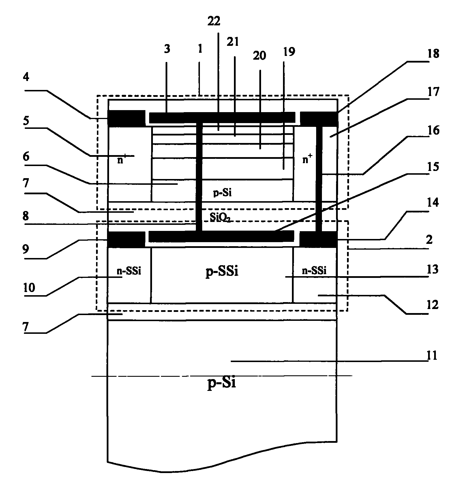
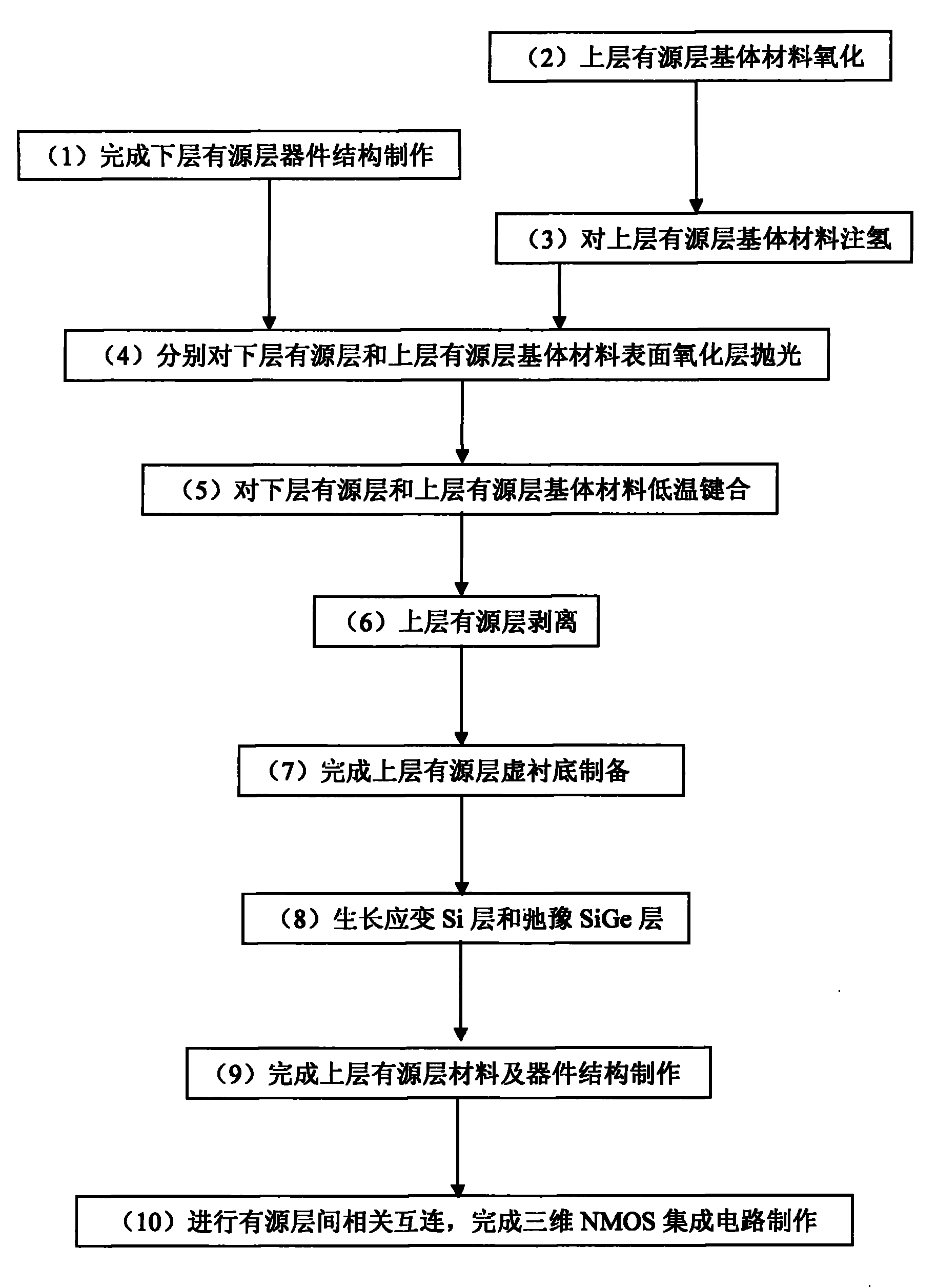
[0039] Embodiment 1: the steps of making a three-dimensional quantum well NMOS integrated device with a conductive channel of 90nm are as follows:

[0040] (1) Select SSOI substrates with stress>1Gpa;

[0041] (2) On the SSOI substrate, use oxidation-photolithography source, drain, gate region-gate oxidation-deposit polysilicon-photolithography polysilicon and diffusion layer contact hole-deposition polysilicon-photolithography polysilicon-phosphorus implantation-low temperature deposition Product SiO 2 - Lithographic wiring holes - polysilicon wiring - low temperature deposition of SiO 2 For the dielectric layer, make a strained Si nMOSFET device structure and interconnection with a conductive channel of 90nm, and complete the lower active layer structure;

[0042] (3) Deposit SiO on the surface of the above active layer 2 medium layer;

[0043] (4) Carry out surface oxidation to the cleaned p-type Si sheet, as the upper substrate material;

[0044] (5) Using an ion impl...

Embodiment 2

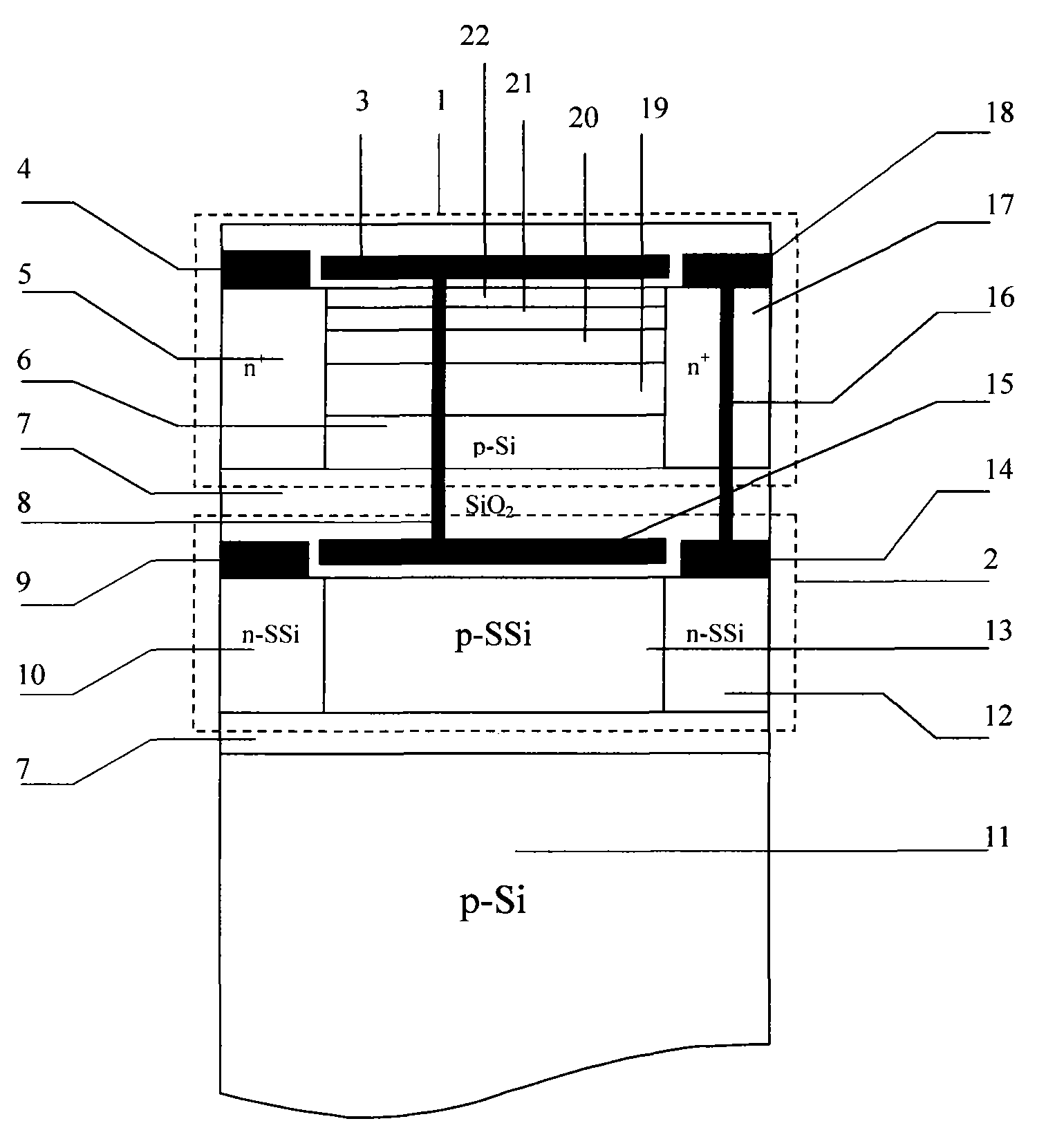
[0052] Embodiment 2: the steps of making a three-dimensional quantum well NMOS integrated device with a conductive channel of 130nm are as follows:

[0053] (1) Select SSOI substrates with stress>1Gpa;

[0054] (2) On the SSOI substrate, use oxidation-photolithography source, drain, gate region-gate oxidation-deposit polysilicon-photolithography polysilicon and diffusion layer contact hole-deposition polysilicon-photolithography polysilicon-phosphorus implantation-low temperature deposition Product SiO 2 - Lithographic wiring holes - polysilicon wiring - low temperature deposition of SiO 2 For the dielectric layer, make a strained Si nMOSFET device structure and interconnections with a conductive channel of 130nm, and complete the lower active layer structure;

[0055] (3) Deposit SiO on the surface of the above active layer 2 medium layer;

[0056] (4) Carry out surface oxidation to the cleaned p-type Si sheet, as the upper substrate material;

[0057] (5) Using an ion i...

Embodiment 3

[0065] Embodiment 3: the steps of making a three-dimensional quantum well NMOS integrated device with a conductive channel of 65nm are as follows:

[0066] (1) Select SSOI substrates with stress>1Gpa;

[0067] (2) On the SSOI substrate, use oxidation-photolithography source, drain, gate region-gate oxidation-deposit polysilicon-photolithography polysilicon and diffusion layer contact hole-deposition polysilicon-photolithography polysilicon-phosphorus implantation-low temperature deposition Product SiO 2 - Lithographic wiring holes - polysilicon wiring - low temperature deposition of SiO 2 For the dielectric layer, make a strained Si nMOSFET device structure and interconnections with a conductive channel of 65nm, and complete the lower active layer structure;

[0068] (3) Deposit SiO on the surface of the above active layer 2 medium layer;

[0069] (4) Carry out surface oxidation to the cleaned p-type Si sheet, as the upper substrate material;

[0070] (5) Using an ion imp...


PUM


Abstract

The invention discloses a 3D quantum well NMOS integrated device and a manufacturing method thereof, relates to the technical field of microelectronics, and mainly solves the problem of low speed of the existing 3D integrated circuits. The proposal is that an SSOI substrate and an SGOI substrate are respectively employed to construct two active layers of a new 3D integrated device; wherein, the lower active layer is the SSOI substrate and is made into strained Si NMOSFET by utilizing the characteristic of high electron mobility of a strained Si material in the SSOI substrate; the upper activelayer is the SGOI substrate on which a strained Si / relaxed SiGe double-layer structure grows and is made into strained Si quantum well channel NMOSFET; the lower active layer and the upper active layer are connected by an interconnection line to form the 3D quantum well NMOS integrated device with a conducting channel of 65nm to 130nm. Compared with the existing 3D integrated devices, the 3D quantum well NMOS integrated device manufactured by the manufacturing method has the advantages of high speed and good performance, and can be applied to manufacturing large-scale and high-speed 3D CMOS integrated circuits.

Description

technical field [0001] The invention belongs to the technical field of semiconductor integrated circuits, in particular to a three-dimensional quantum well NMOS integrated device and a manufacturing method thereof. Background technique [0002] Since the 1960s, the feature size of integrated circuits has been continuously reduced following Moore's Law, and the integration and performance of chips have been continuously improved. Entering the deep submicron era, the interconnection of devices inside the chip becomes more and more complex. Therefore, the influence of the delay time caused by the parasitic resistance and parasitic capacitance of the interconnection on the performance of the circuit becomes more and more prominent. Studies have shown that after the feature size of the device is less than 250nm, the R-C delay caused by conventional metal wiring will dominate the entire circuit delay, which restricts the continuous improvement of VLSI integration and performance....

Claims


Application Information

Patent Timeline
Patent Type & Authority Patents(China)
IPC IPC(8): H01L27/12H01L21/84
Inventor 张鹤鸣胡辉勇宣荣喜戴显英舒斌宋建军徐小波
Owner XIDIAN UNIV
Why Eureka
Try Eureka