
Gamma gate heterojunction field effect transistor and preparation method thereof

A heterojunction field effect and transistor technology, applied in the field of microelectronics, can solve the problems of reducing the stability of the device, reducing the yield of the device, increasing the feedback capacitance of the device, etc., to reduce the gate leakage current, improve the breakdown voltage, Reduce the effect of gate leakage

Active Publication Date: 2009-04-22
云南凝慧电子科技有限公司
View PDF0 Cites 5 Cited by
  • Summary
  • Abstract
  • Description
  • Claims
  • Application Information

AI Technical Summary

Problems solved by technology

However, the manufacturing process of the heterojunction field effect transistor using the stacked field plate structure is relatively complicated. Each additional layer of field plate requires additional process steps such as photolithography, metal deposition, insulating dielectric material deposition, stripping, and cleaning. To make the insulating dielectric material deposited under the field plates of each layer have an appropriate thickness, cumbersome process debugging must be carried out, which greatly increases the difficulty of device manufacturing and reduces the yield of devices.
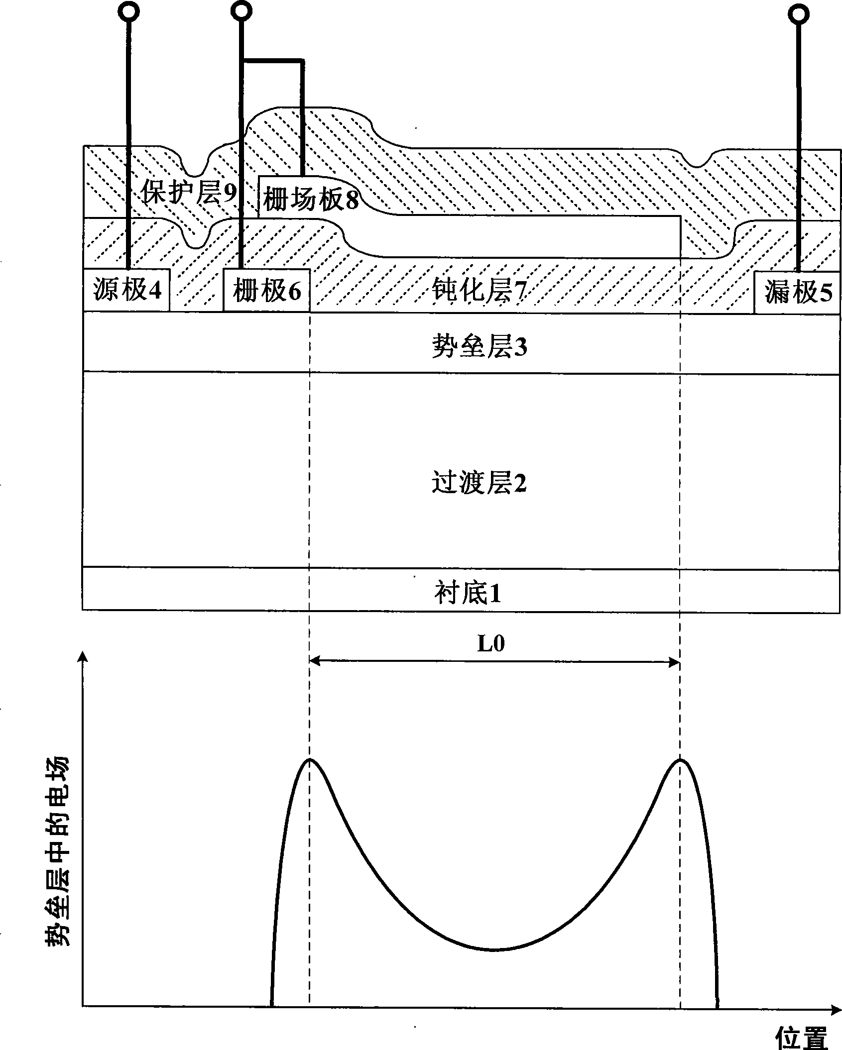
Another issue worthy of people's attention is that all heterojunction field effect transistors with a gate field plate structure will generate additional capacitance between the gate field plate and the two-dimensional electron gas channel, which will be superimposed into the gate of the device In the feedback capacitance between the drain and the drain, the feedback capacitance of the device increases, resulting in a certain attenuation of the power characteristics and frequency characteristics of the device
In addition, the increase of the feedback capacitance of the device will weaken the isolation between the input and output of the device and reduce the stability of the device

Method used


Image

  • Gamma gate heterojunction field effect transistor and preparation method thereof
  • Gamma gate heterojunction field effect transistor and preparation method thereof
  • Gamma gate heterojunction field effect transistor and preparation method thereof

Examples


Embodiment 1

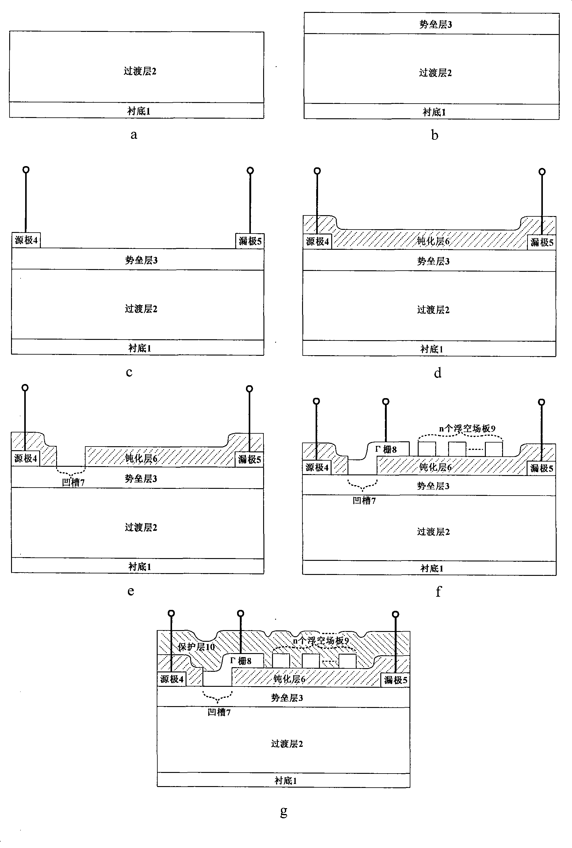
[0054] The production substrate is sapphire, and the passivation layer is SiO 2 , the protective layer is SiO 2 , the Γ gate and each floating field plate are Mo / Au metal combination Γ gate heterojunction field effect transistors, the process is:

[0055] 1. Using metal organic chemical vapor deposition technology to epitaxially undoped transition layer 2 with a thickness of 1 μm on the sapphire substrate 1, the transition layer is composed of AlN material with a thickness of 37 nm and GaN material with a thickness of 0.963 μm from bottom to top constitute. The process conditions used for the epitaxial lower layer AlN material are: temperature 595 ° C, pressure 170 Torr, hydrogen gas flow rate 4800 sccm, ammonia gas flow rate 4800 sccm, aluminum source flow rate 40 μmol / min; the process conditions used for the epitaxial upper layer GaN material are: temperature 1060°C, pressure 170 Torr, hydrogen flow rate 4800 sccm, ammonia gas flow rate 4800 sccm, gallium source flow rate 17...

Embodiment 2

[0063] The substrate is silicon carbide, the passivation layer is SiN, the protective layer is SiN, the Γ gate and each floating field plate are Ni / Au metal combination Γ gate heterojunction field effect transistor, and the process is:

[0064] 1. An undoped transition layer 2 with a thickness of 1.5 μm is epitaxially formed on a silicon carbide substrate 1 by metal-organic chemical vapor deposition technology. Made of GaN material. The process conditions used for the epitaxial lower layer AlN material are: temperature 1030°C, pressure 175 Torr, hydrogen gas flow rate 4900 sccm, ammonia gas flow rate 4900 sccm, aluminum source flow rate 14 μmol / min; the process conditions for the epitaxial upper layer GaN material are: temperature 1030°C, pressure 175 Torr, hydrogen flow rate 4900 sccm, ammonia gas flow rate 4900 sccm, gallium source flow rate 170 μmol / min.

[0065] 2. Deposit an undoped barrier layer 3 with a thickness of 30nm on the GaN transition layer 2 by metal organic c...

Embodiment 3

[0072] The production substrate is silicon, the passivation layer is SiN, and the protective layer is Al 2 o 3 , the Γ gate and each floating field plate are Pt / Au metal combined Γ gate heterojunction field effect transistors, and the process is:

[0073] 1. Using metal organic chemical vapor deposition technology to epitaxially undoped transition layer 2 with a thickness of 5 μm on the silicon substrate 1, the transition layer is composed of AlN material with a thickness of 130 nm and GaN material with a thickness of 4.87 μm from bottom to top constitute. The process conditions used for the epitaxial lower layer AlN material are: temperature 870°C, pressure 178 Torr, hydrogen gas flow rate 5000 sccm, ammonia gas flow rate 5000 sccm, aluminum source flow rate 40 μmol / min; the process conditions for the epitaxial upper layer GaN material are: temperature 1060°C, pressure 178 Torr, hydrogen flow rate 5000 sccm, ammonia gas flow rate 5000 sccm, gallium source flow rate 170 μmol...


PUM


Abstract

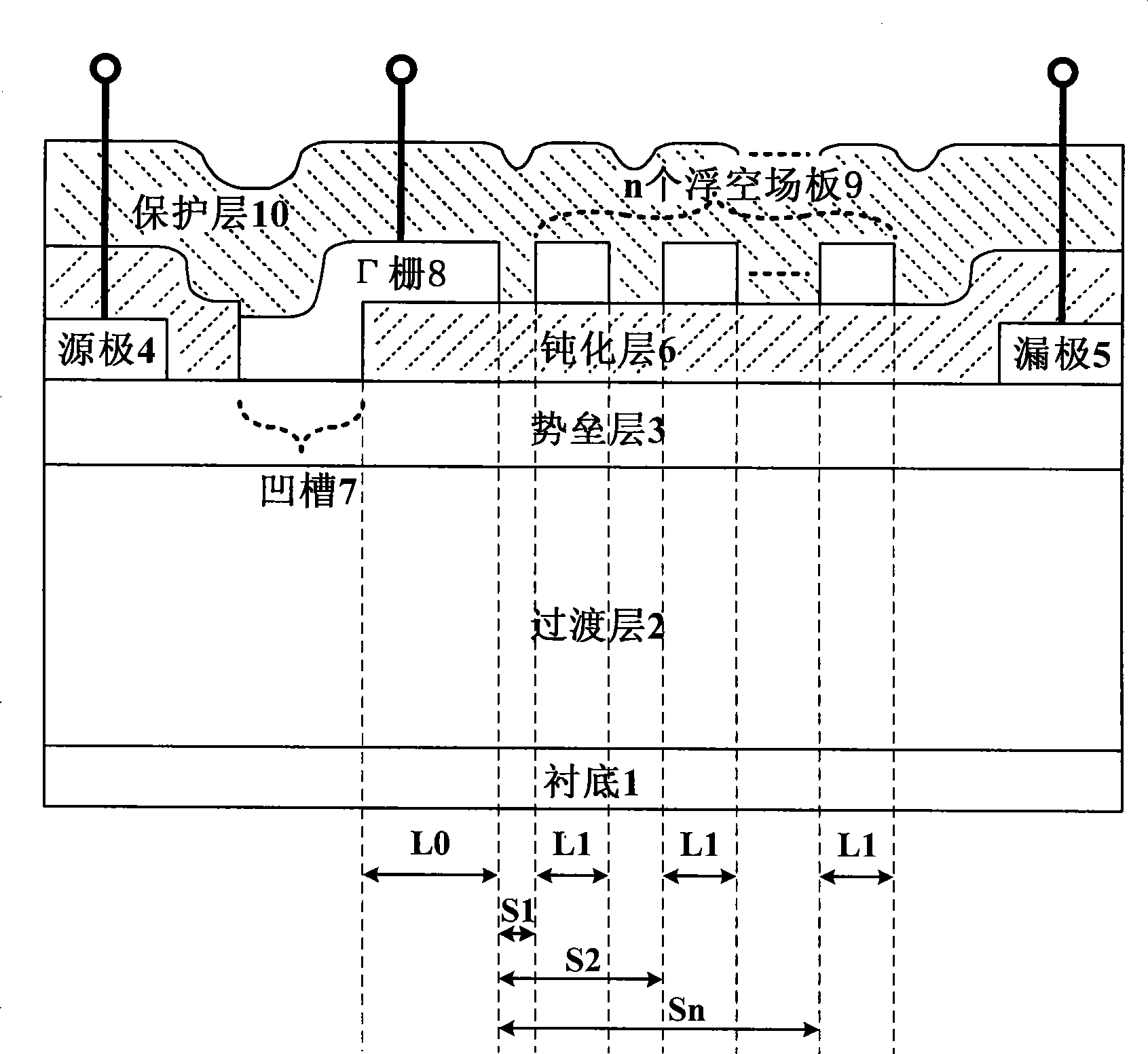
The invention discloses a gamma gate heterojunction field effect transistor and a fabrication method thereof. The transistor comprises, from bottom to top, a substrate (1), a transition layer (2), a barrier layer (3), a source electrode (4), a drain electrode (5), a passivation layer (6), a gamma gate (8) and a protection layer (10); a groove (7) is opened on the passivation layer (6), wherein, n floating field plates (9) are deposited on the passivation layer (6) arranged between the gamma gate (8) and drain electrode (5) to form a composite gate field plate structure (n is not less than 1). All the floating field plates have the same size and are mutually independent, and the distance between two adjacent floating field plates increases based on the number of the floating field plates arranged along the direction from the gamma gate to the drain electrode. The n floating field plates are in a floating state and completed together with the gamma gate by one-time process. The transistor has the advantages of simple process, good reliability, strong stability, good frequency characteristic and high output power, and the transistor and the fabrication method can be used for fabricating high-frequency high power devices based on III-V group compound semiconductor heterojunction structure.

Description

technical field [0001] The invention belongs to the field of microelectronics technology, and relates to semiconductor devices, especially a Γ-gate heterojunction field-effect transistor based on the heterojunction structure of III-V compound semiconductor materials, which can be used as a basic device for microwave, millimeter wave communication systems and radar systems . technical background [0002] As is well known in the industry, semiconductor materials composed of group III elements and group V elements, that is, group III-V compound semiconductor materials, such as gallium nitride (GaN)-based, gallium arsenide (GaAs)-based, indium phosphide (InP)-based And other semiconductor materials, their bandgap widths are often quite different, so people usually use these III-V compound semiconductor materials to form various heterojunction structures. Due to the large difference in the band gap of III-V compound semiconductor materials on both sides of the heterojunction int...

Claims


Application Information

Patent Timeline
Patent Type & Authority Applications(China)
IPC IPC(8): H01L29/772H01L29/06H01L21/335
Inventor 郝跃过润秋毛维杨翠
Owner 云南凝慧电子科技有限公司
Learn More