Cleaning method after opening etching

An etching and wet cleaning technology, which is applied in the fields of electrical components, semiconductor/solid-state device manufacturing, circuits, etc., can solve the problems of damaging the low dielectric constant dielectric layer, changing, and reducing the process capacity, so as to improve the process yield and simplify the process. Process steps, the effect of reducing process costs

Inactive Publication Date: 2009-06-10
UNITED MICROELECTRONICS CORP
View PDF2 Cites 19 Cited by
  • Summary
  • Abstract
  • Description
  • Claims
  • Application Information

AI Technical Summary

Problems solved by technology

[0008] However, the above use contains both hydrogen/oxygen/carbon tetrafluoride (CF 4 ) plasma cleaning method, or only hydrogen plasma cleaning method, but still cannot effectively remove the residual polymer or metal residue, so it has not been able to make a breakthrough in increasing the process yield (yield)
Therefore, after the known plasma cleaning method, it is often necessary to use multiple wet cleaning processes to remove these residual polymers or metal residues; howe...

Method used


Image

  • Cleaning method after opening etching
  • Cleaning method after opening etching
  • Cleaning method after opening etching

Examples


Embodiment Construction

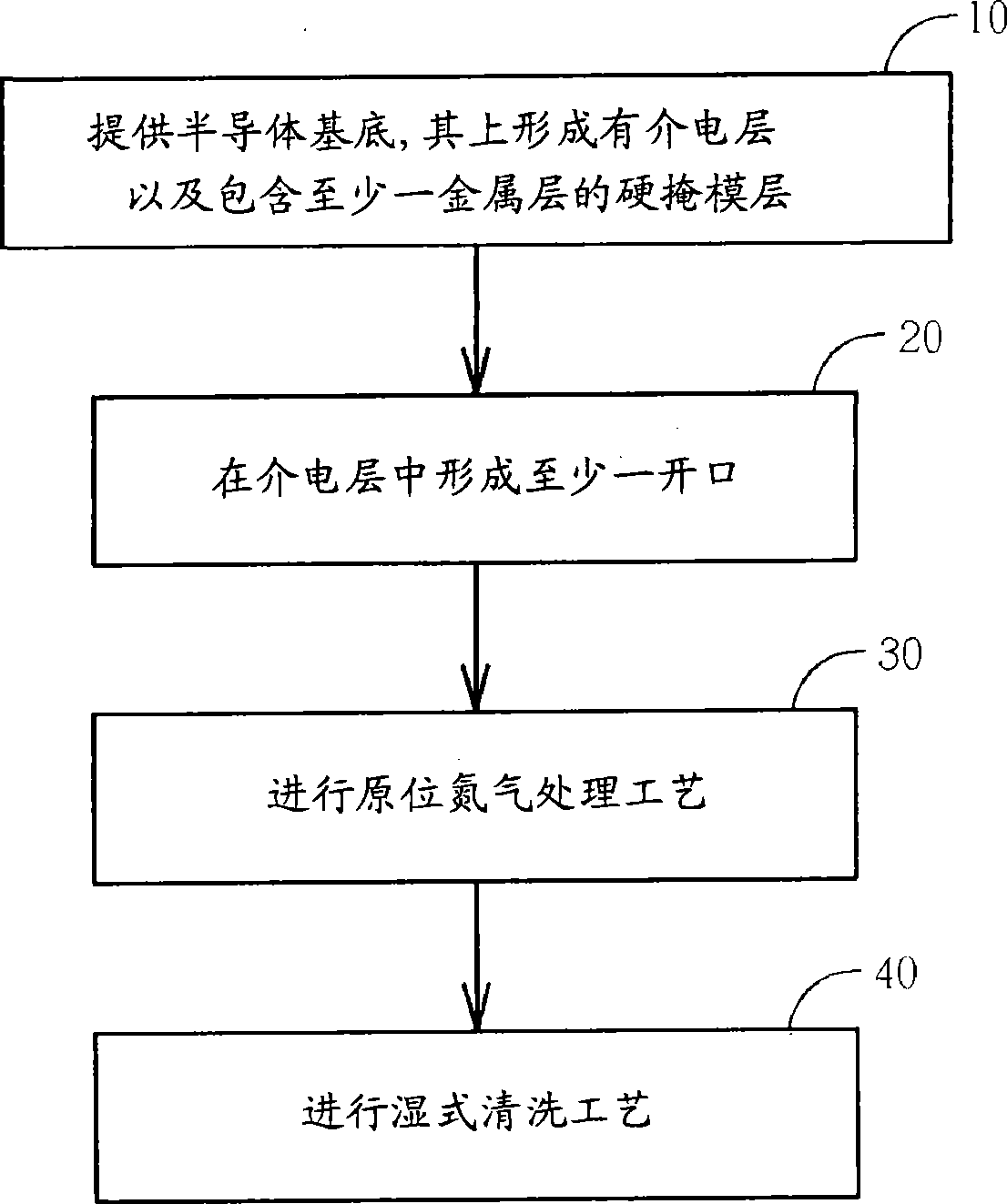
[0037] Please refer to figure 1 , figure 1 It is a flowchart of the cleaning method after opening etching in the present invention. Such as figure 1As shown, in step 10, first provide a semiconductor substrate, such as a silicon substrate or a silicon-on-insulator (SOI) substrate, etc., on which a dielectric layer and a hard mask layer are formed, wherein the hard The mask layer includes at least one metal layer. The semiconductor substrate may also include at least one functional element, such as a Metal Oxide Semiconductor (MOS) transistor. The dielectric layer is a low dielectric constant dielectric layer, such as carbon-doped oxide (carbon-doped oxide; CDO), organic silicon glass (OSGs), fluorine-containing silicon dioxide (FSGs), or ultra-low dielectric constant ( Ultra low-k; k<2.5) and other material layers; methods for forming low-k dielectric layers include spin-coating (spin-coating) process, plasma-enhanced chemical vapor deposition (plasma-enhanced chemical vap...


PUM


Abstract

The invention provides a washing method after etching openings. The method comprises the steps of providing a semiconductor substrate with a dielectric layer, etching openings to form at least one opening in the dielectric layer, carrying out a nitrogen treatment process to wash C-F polymer residue in the opening and finally carrying out a wet washing process.

Description

technical field [0001] The invention provides a cleaning method after opening etching, especially a cleaning method using an in-situ nitrogen treatment process. Background technique [0002] Copper dual damascene (dual damascene) technology with low dielectric constant (low-k; k≤2.9) dielectric layer is currently known as the best metal inner layer for high-integration, high-speed logic integrated circuit chip manufacturing and semiconductor processes below 0.13 microns Wired solutions. The reason is that copper has low resistance value (30% lower than aluminum) and preferred anti-electro-migration resistance (electro-migration resistance), and the dielectric layer material with low dielectric constant can help reduce the resistance between metal wires - Capacitance Time Delay (Resistance-Capacitance Time Delay), it can be seen that the dielectric layer material with low dielectric constant and the copper metal dual damascene interconnection technology are increasingly impo...

Claims


Application Information

Patent Timeline
IPC IPC(8): H01L21/768H01L21/3105
Inventor 王界入姚志成赖育聪廖俊雄
Owner UNITED MICROELECTRONICS CORP
Why Eureka
Try Eureka