

Insulating layer, electronic device, field effect transistor, and polyvinylthiophenol
一种聚乙烯基苯硫酚、场效应晶体管的技术,应用在晶体管、电气元件、电固体器件等方向,能够解决未表现出元件特性等问题,达到改善迁移度、改善元件特性的效果
- Summary
- Abstract
- Description
- Claims
- Application Information
AI Technical Summary
Problems solved by technology
Method used
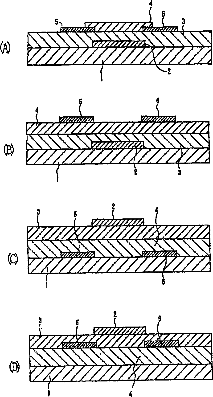
Image

Examples
Embodiment
[0183] Hereinafter, the present invention will be described in detail through examples. These examples are for illustrating the present invention. The present invention is not limited to the following examples, and can be implemented with any modifications within the scope not departing from the gist thereof.
Synthetic example 1
[0184] [Synthesis Example 1: Synthesis of p-vinylbenzenethiol]
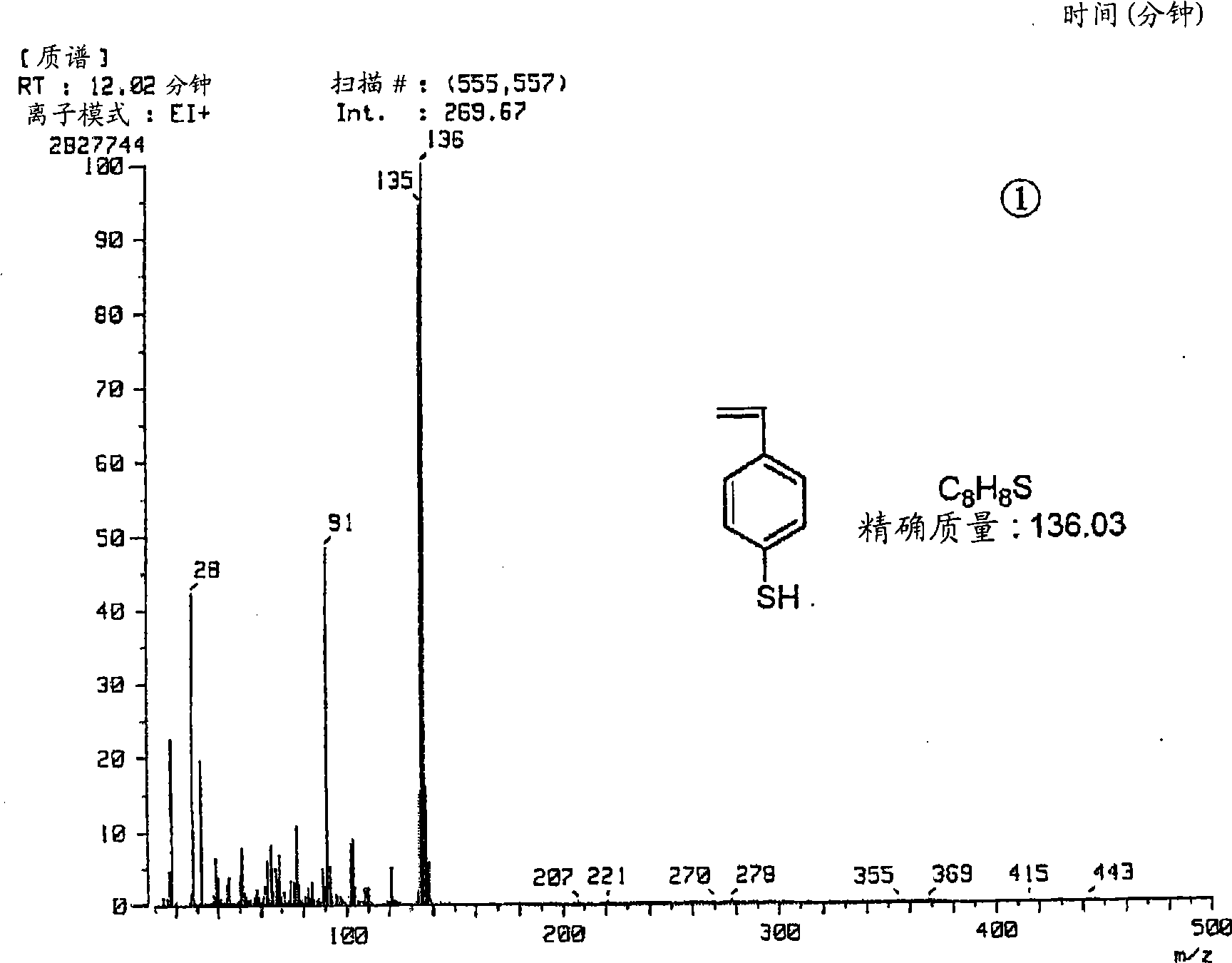
[0185] 1.64 g of Mg powder was dispersed in 53 mL of tetrahydrofuran (THF) at room temperature under a nitrogen atmosphere, and 8 mL of 4-bromostyrene (manufactured by Aldrich) was slowly added dropwise. In order to suppress the rise of the heat of reaction during the reaction, it was cooled stepwise to -15°C to prepare a Grignard reaction solution. While maintaining this temperature, sulfur powder (manufactured by Aldrich) was added to the reaction liquid, and the temperature was gradually returned to 0° C. over 3 hours. After 3 hours, 1N NaOH aqueous solution was added to the reaction liquid, followed by stirring. The reaction liquid was filtered off, and liquid separation was carried out with ether. The aqueous layer was collected and concentrated under reduced pressure at room temperature. 1N HCl was slowly added to the aqueous layer, and when the pH was adjusted to 6.5, the aqueous layer was pale yellow. ...
Synthetic example 2
[0190] [Synthesis Example 2: Protection of Thiol by Acetyl Group]
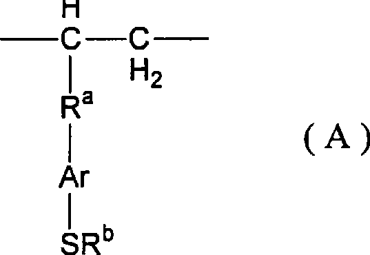
[0191] 2.7 g of p-vinylbenzenethiol obtained in Synthesis Example 1 was dissolved in 300 mL of THF at -5°C under a nitrogen atmosphere, and 10 mL of pyridine was added as a deoxidizer. After stirring well for 1 hour, 3 g of acetyl chloride was slowly added dropwise. After the dropwise addition was completed, the mixture was stirred for 1 hour, and pyridine hydrochloride was precipitated. The pyridine hydrochloride was filtered off, the filtrate was concentrated under reduced pressure at low temperature, and liquid separation and extraction were performed with benzene and water, and the organic layer was concentrated under reduced pressure at low temperature to obtain a light yellow liquid. This liquid was purified by alumina column chromatography (dichloromethane) to obtain p-vinylbenzenemercaptan having an acetyl-protecting group as the target product.
[0192] In addition, the obtained products were measur...
PUM
| Property | Measurement | Unit |
|---|---|---|
| electrical conductivity | aaaaa | aaaaa |
| glass transition temperature | aaaaa | aaaaa |
| glass transition temperature | aaaaa | aaaaa |
Abstract
Description
Claims
Application Information