

Titanium dioxide thin film with dual-layer nano-ordered structure and preparation method thereof
A titanium dioxide and ordered structure technology is applied in the field of double-layer nano-ordered structure titanium dioxide film and its preparation, and can solve the problems of inability to uniformly cover the nano-ordered array film and the like
- Summary
- Abstract
- Description
- Claims
- Application Information
AI Technical Summary
Problems solved by technology
Method used
Image

Examples
Embodiment 1
[0021] 1) Mix hydrofluoric acid with a concentration of 50%, nitric acid with a concentration of 68%, and deionized water in a volume ratio of 1:3:6 to obtain a pickling solution;
[0022] 2) Dissolving 100 mg of hexamethylene in 50 ml of a mixed solution of 30% hydrogen peroxide and 1.0 ml of 63% nitric acid. Set the size to 5×5×0.01(cm 3 ) on the surface of the metal titanium plate was pickled with the pickling solution obtained in step 1) at a temperature of 60°C, then ultrasonically cleaned with deionized water, immersed in the above mixed solution, and reacted at 80°C for 48 hours to take out the metal Titanium plate, centrifuge the reaction solution, remove the suspended powder, and obtain the precursor containing tetravalent titanium ions;
[0023] 3) Another size is 5×5×0.01(cm 3 ) metal titanium plate, pickling the surface with the pickling solution obtained in step 1) at a temperature of 60° C., then ultrasonically cleaning it with deionized water, and then immersi...
Embodiment 2
[0028] The preparation method is the same as in Example 1. The difference is: the anodizing voltage is 25V, and the oxidation time is 15 minutes.
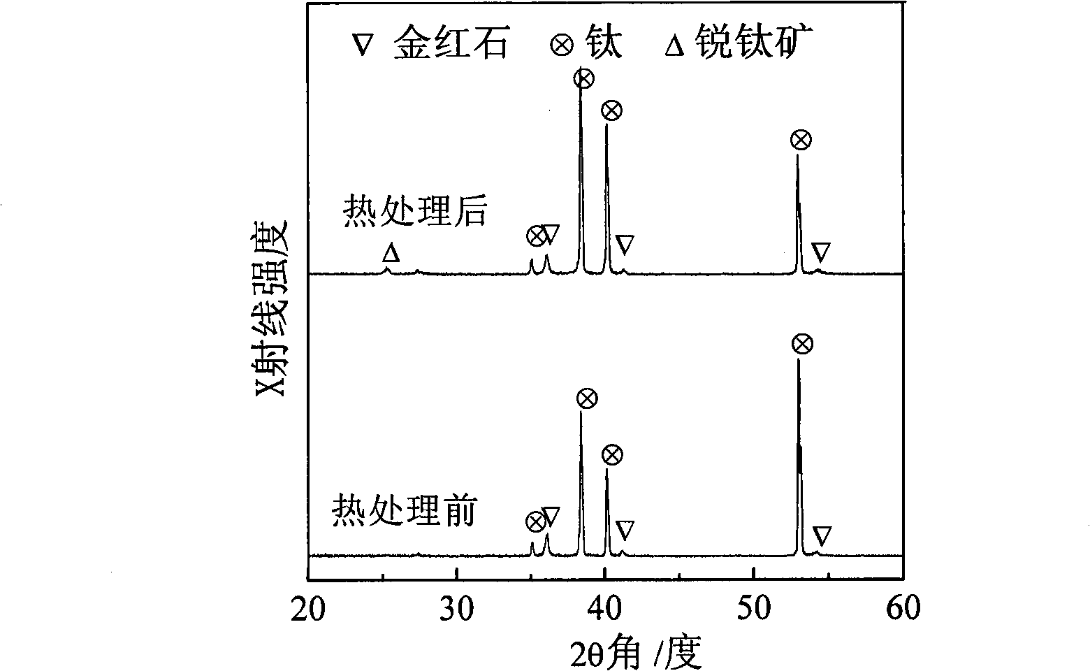
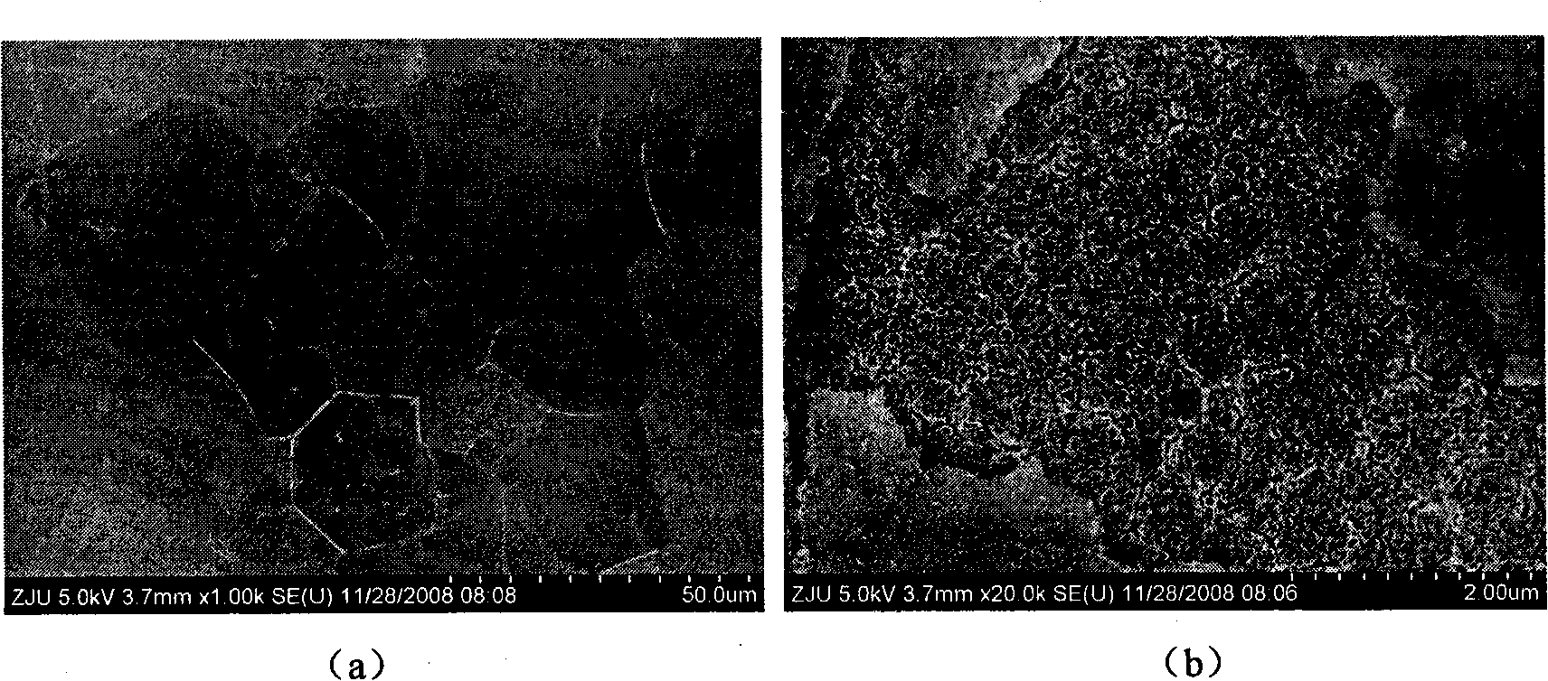
[0029] Structural characterization of double-layer nano-ordered titanium dioxide film:
[0030] image 3 (a) shows that the double-layer film is overall uniform, and the short rutile nanorod arrays are quasi-oriented. The short rods have a diameter of about 40 nm and a length of about 150 nm. image 3 (b) shows that the anatase nanotubes are arranged regularly and oriented, with an average diameter of 50 nm and a wall thickness of about 12 nm. The overall thickness of the film is about 700nm, the upper layer is rutile phase, and the lower layer is anatase phase.
Embodiment 3
[0032] The preparation method is the same as in Example 1. The difference lies in: step 3) the reaction time for immersing the metal titanium plate in the precursor is 48 hours, step 4) anodic oxidation voltage 25V, oxidation time 15 minutes.
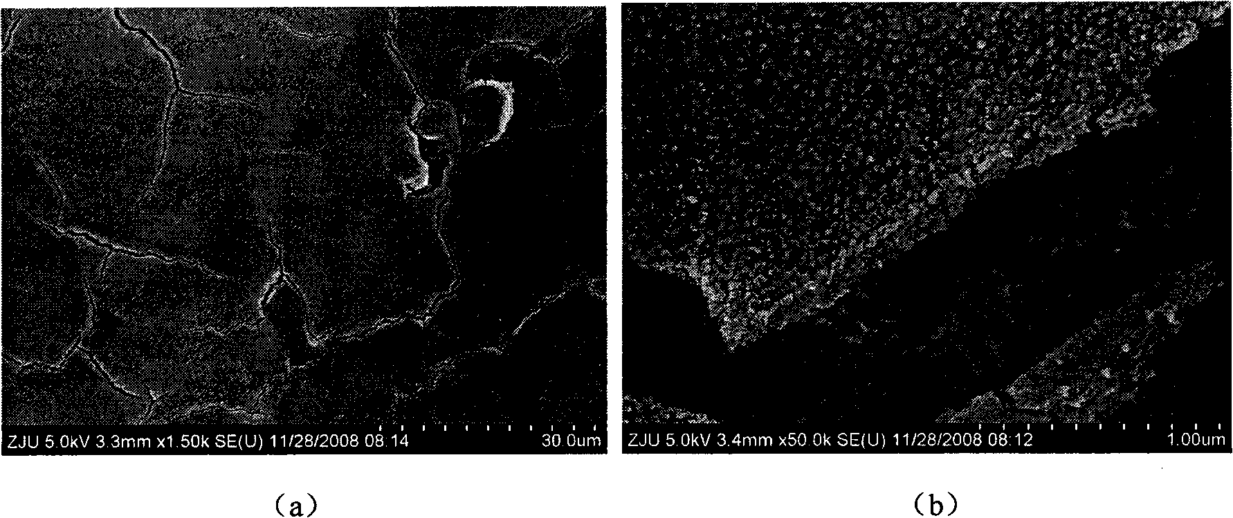
[0033] Structural characterization of double-layer nano-ordered titanium dioxide film:
[0034] Figure 4 (a) shows that the double-layer film is overall uniform, and the short rutile nanorod arrays are quasi-oriented. The diameter of the short rods is about 100 nm, and the length is about 250 nm. Figure 4b shows that the anatase nanotubes are regularly arranged, with an average diameter of 100 nm and a wall thickness of about 15 nm. The overall thickness of the film is about 1000nm, the upper layer is rutile phase, and the lower layer is anatase phase.
PUM
| Property | Measurement | Unit |
|---|---|---|
| thickness | aaaaa | aaaaa |
| diameter | aaaaa | aaaaa |
| length | aaaaa | aaaaa |
Abstract
Description
Claims
Application Information