
External cavity type multiple-active region photon crystal vertical cavity surface transmission semiconductor laser device

A vertical cavity surface emission and photonic crystal technology, applied in the field of optoelectronics, can solve the problems of increased threshold current, large light emitting area, and large series resistance, etc., and achieve the goals of reducing series resistance, increasing light emitting area, and strong anti-interference ability Effect

Inactive Publication Date: 2009-11-25
BEIJING UNIV OF TECH
View PDF0 Cites 7 Cited by
  • Summary
  • Abstract
  • Description
  • Claims
  • Application Information

AI Technical Summary

Problems solved by technology

This kind of laser generally has the following disadvantages: 1. The single-pass optical gain of ordinary vertical cavity surface emitting semiconductor lasers is small. In order to increase the output power, the method of increasing the light output area or increasing the current injection is generally adopted.
Using the method of increasing the light output area will make the distribution of the carrier density in the active area worse, and the center current density will become smaller, which will increase the threshold current; when using large current injection, the carrier distribution in the active area will appear space burning. Holes, which affect the distribution of gain and refractive index, appear multi-transverse mode lasing
In addition, the thermal stability of the device deteriorates under the condition of high current injection
2. In order to achieve single-mode operation, the carrier density distribution in the central part of the active region must be relatively uniform, and it is difficult to achieve single-mode operation if the light output area is too large
3. Smaller oxidation holes will inevitably cause large series resistance, and it is difficult to control the process of making small oxidation holes
Single-mode output power is low and threshold current is large

Method used


Image

  • External cavity type multiple-active region photon crystal vertical cavity surface transmission semiconductor laser device
  • External cavity type multiple-active region photon crystal vertical cavity surface transmission semiconductor laser device
  • External cavity type multiple-active region photon crystal vertical cavity surface transmission semiconductor laser device

Examples


specific Embodiment approach

[0027] Specific implementation methods (taking the wavelength 850nm as an example)

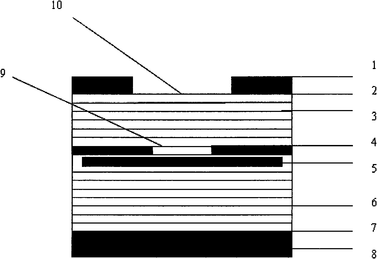
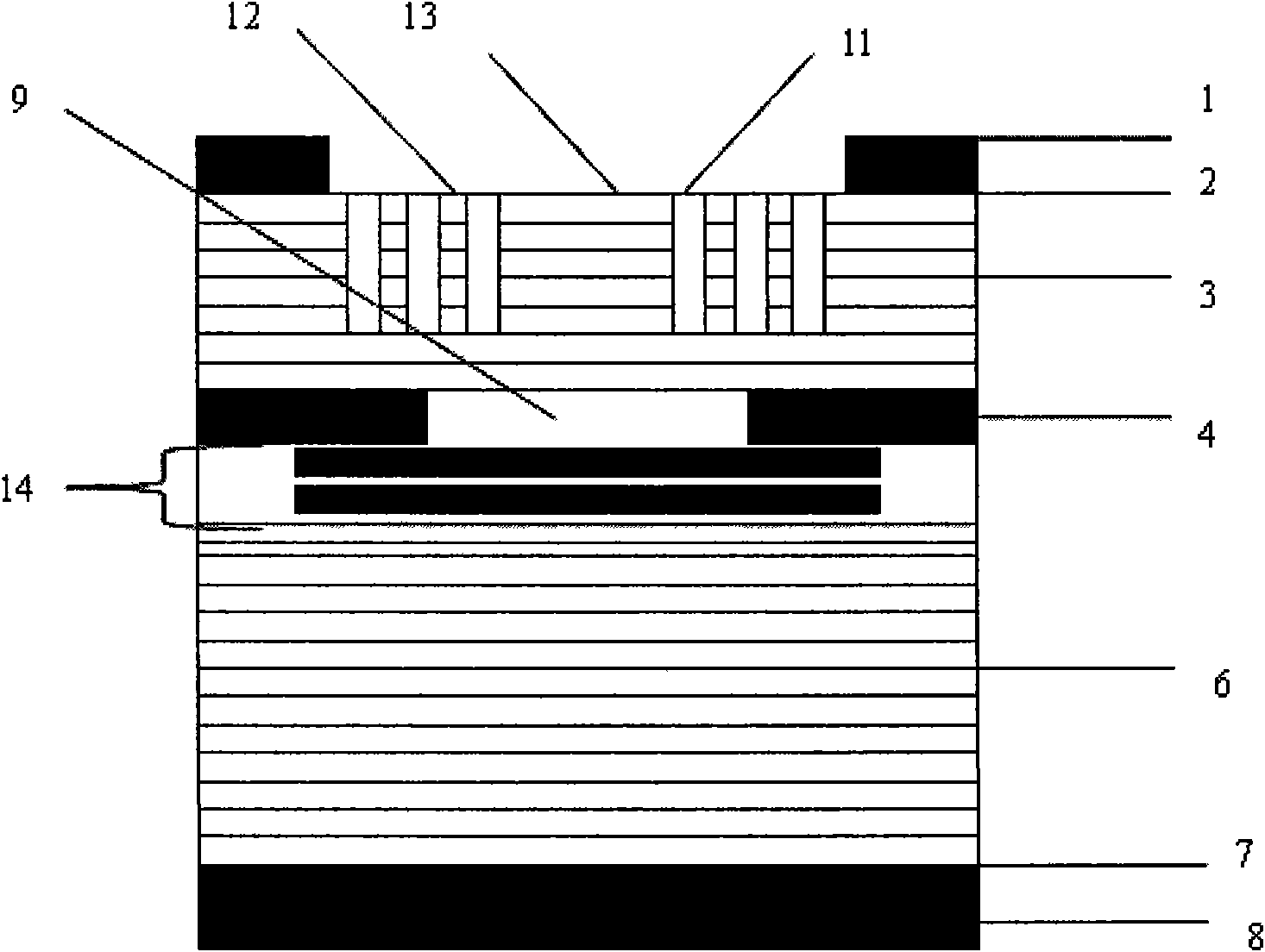
[0028] 1. Pass in N + The substrate 7 was obtained by growing on a GaAs substrate of type 1, and then a 0.3 micron GaAs buffer layer was grown on the substrate by MOCVD method, and then N + al 0.1 Ga 0.9 As (60nm doping concentration 3×10 18 cm -3 ) and n + al 0.9 Ga 0.1 As (68.19nm doping concentration 3×10 17 cm -3 ) composed of 28 cycles of the lower DBR6, In 0.18 al 0.12 Ga 0.7 As and Al 0.22 Ga 0.78 AS composed of single active region 5 heavily doped N + GaAs and P + Multiple active regions (three active regions) cascaded with GaAs reverse tunnel junctions 14, Al 0.98 Ga 0.02 As (30nm doping concentration 1×10 18 cm -3 ) oxidation limiting layer 4,, Al 0.1 Ga 0.9 As (60nm doping concentration 3×10 18 cm -3 ) and Al 0.9 Ga 0.1 As (68.19nm doping concentration 3×10 18 cm -3 ) consisting of 24 cycles of upper DBR3, Al 0.1 Ga 0.9 As heavily doped ohmic contact lay...


PUM


Abstract

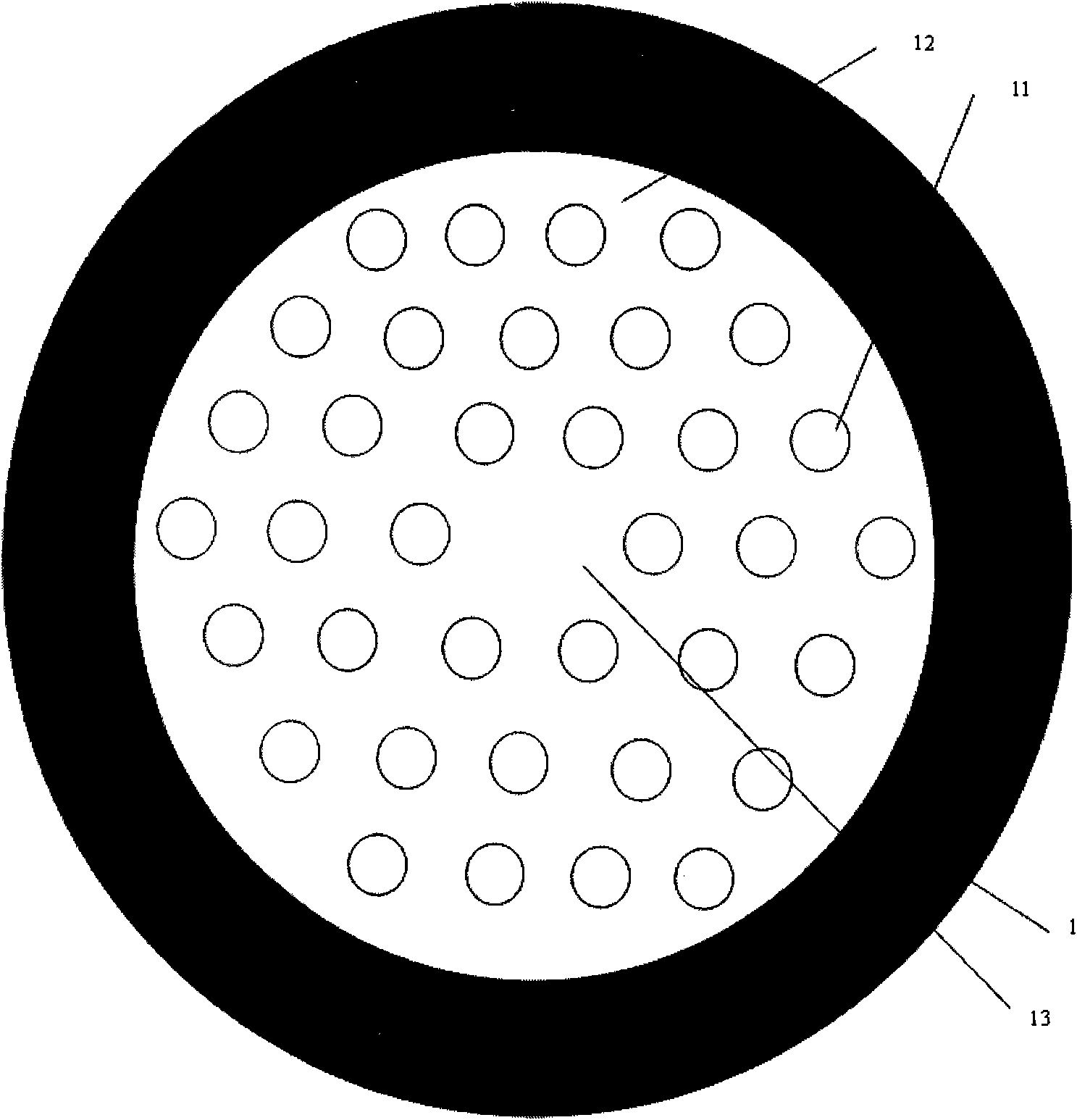
An external cavity type multiple-active region photon crystal vertical cavity surface transmission semiconductor laser device belongs to the semiconductor photoelectron field. The common oxidation limiting vertical cavity surface transmission semiconductor laser device has problems of small single pass light gain, multiple-transverse module laser shooting, low single module output power, large threshold current and large series resistance and so on. The invention adopts the multiple-active region structure on the active region of the device, meanwhile leads the defect type photon crystal structure into DBR on the vertical cavity surface transmission semiconductor laser device, the external cavity type multiple-active region photon crystal vertical cavity surface transmission semiconductor laser device with dozens of micrometres of single module operation oxidation bore diameter, dozens of mws of single module power, dozens of Ohms of series resistances and more than 35 dbs of side module inhibition can be obtained by optimizing the photon crystal period, the air bore diameter, the etching depth, the device diameter and the oxidation bore diameter and so on reasonably.

Description

technical field [0001] The invention belongs to the technical field of optoelectronics, and in particular relates to the design and manufacture of a novel vertical-cavity surface-emitting semiconductor laser. Suitable for vertical cavity surface emitting semiconductor lasers of various wavelengths (650nm, 850nm, 980nm, etc.). Background technique [0002] Vertical cavity surface emitting lasers (vertical cavity surface emitting lasers, VCSELS) is a semiconductor laser with excellent performance. VCSELS has the characteristics of high coupling efficiency with optical fibers, easy formation of two-dimensional arrays and integration; low threshold, single longitudinal mode, high modulation speed; reliability and high cost performance. It has good application prospects in high-density area array, optical network, data transmission, optical interconnection, optical storage, optical computing, etc., and has good application prospects in optical communication local network data co...

Claims


Application Information

Patent Timeline
Patent Type & Authority Applications(China)
IPC IPC(8): H01S5/183H01S5/065H01S5/06H01S5/20
Inventor 沈光地徐晨解意洋陈弘达阚强王春霞刘英明王宝强
Owner BEIJING UNIV OF TECH
Learn More