Graphic substrate for epitaxial growth and production method thereof
A patterned substrate and epitaxial growth technology, which is applied in the manufacture of semiconductor/solid-state devices, electrical components, electrical solid-state devices, etc., can solve the problems of light absorption of Si substrates, which can reduce the difficulty of the manufacturing process and improve the light extraction efficiency. , the effect of releasing thermal stress
- Summary
- Abstract
- Description
- Claims
- Application Information
AI Technical Summary
Problems solved by technology
Method used
Image

Examples
Embodiment 1
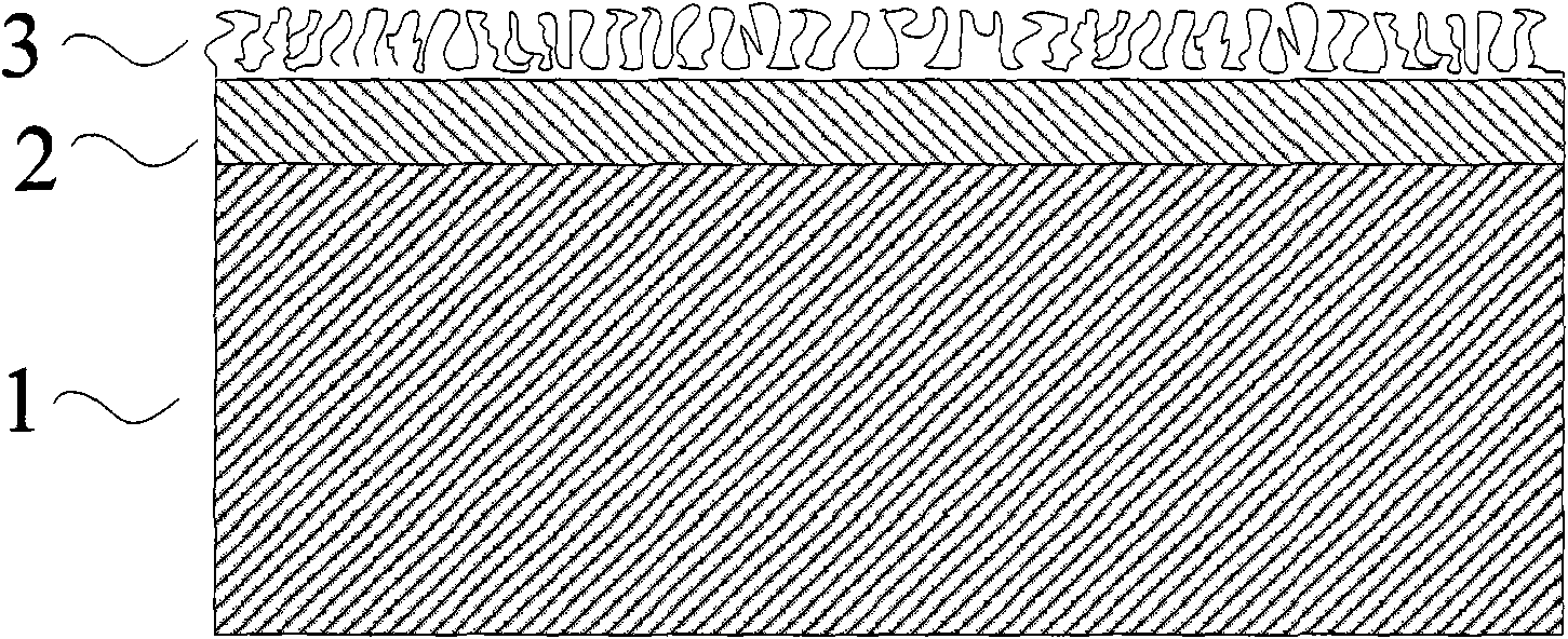
[0023] refer to figure 1 , a schematic side view of a pattern substrate for epitaxial growth, which includes a substrate 1 and an Al layer 2 on the substrate 1, and a sapphire structure layer 3 with a porous pattern structure on the Al layer 2.
[0024] Wherein, the substrate 1 may be Si, may also be an SOI substrate, may also be an AsGa substrate, may also be a GaP substrate, or may be other substrates with large absorption of visible light.
[0025] The thickness of the sapphire structure layer 3 is 100 nm-2 μm, and the thickness of the Al layer 2 is 50 nm-5 μm. The pore diameter of porous alumina is between 5 and 400nm.
[0026] Taking Si substrate as an example, figure 1 The preparation method of the shown pattern substrate comprises the following steps:
[0027] a. First clean the Si substrate 1 with a chemical solution and pure water, ultrasonic cleaning, and prepare an Al layer 2 with a thickness of 100nm to 7μm by electron beam evaporation, ion sputtering, thermal e...
Embodiment 2
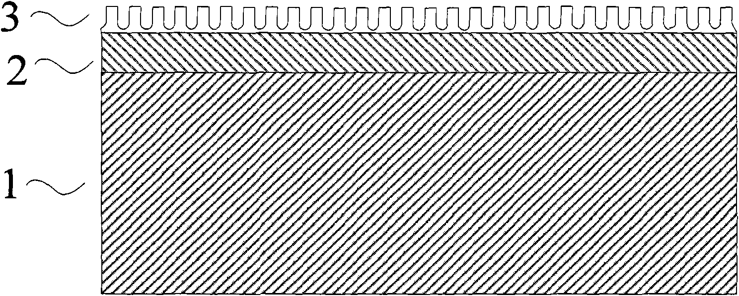
[0034] Such as figure 2 As shown, this embodiment is similar to Embodiment 1, the difference is that in order to prepare a pattern substrate with better periodicity, we adopt the method of secondary anodic oxidation. To achieve this, we inserted the following steps between steps b and c of Example 1:
[0035] Use a certain concentration ratio of HgCl 2 or H 3 PO 4 or HCl or CuCl 2 Or the mixture of the above-mentioned acids, the oxide layer obtained by anodizing once is removed, leaving shallow periodic micropores on the surface, repeating step b of Example 1, and anodizing again to obtain a periodic surface pattern.
Embodiment 3
[0037] Such as figure 2 As shown, this embodiment is similar to Embodiment 1, the difference is that in order to prepare a pattern substrate with better periodicity, we use the pattern preforming method to form a shallower layer on the surface of the Al layer before anodizing the sample. pattern. To achieve this, we inserted the following steps between steps a and b of Example 1:
[0038] Electron beam lithography, multi-beam interference, ion beam etching and other methods are used to fabricate a hard film with a periodic pattern, and then the embossing method is used to form shallow periodic micropores on the surface of the Al layer. This method can form hexagonal lattice, square lattice, triangular lattice and other patterns.
PUM
| Property | Measurement | Unit |
|---|---|---|
| thickness | aaaaa | aaaaa |
| thickness | aaaaa | aaaaa |
| thickness | aaaaa | aaaaa |
Abstract
Description
Claims
Application Information
 - R&D
- Intellectual Property
- Life Sciences
- Materials
- Tech Scout
- Unparalleled Data Quality
- Higher Quality Content
- 60% Fewer Hallucinations
Browse by: Latest US Patents, China's latest patents, Technical Efficacy Thesaurus, Application Domain, Technology Topic, Popular Technical Reports.
© 2025 PatSnap. All rights reserved.Legal|Privacy policy|Modern Slavery Act Transparency Statement|Sitemap|About US| Contact US: help@patsnap.com