High-k gate dielectric material and preparation method thereof

A technology of gate dielectric and thin film, applied in the field of high-k gate dielectric material and its preparation, amorphous Er2O3-Al2O3 high-K gate dielectric composite oxide thin film, which can solve the problem of low crystallization temperature, increased diffusion of impurities at grain boundaries, leakage High crystallization temperature, good flatness, and wide band gap can be achieved without problems such as current increase

Inactive Publication Date: 2010-01-27
SHAOXING UNIVERSITY
View PDF0 Cites 5 Cited by
  • Summary
  • Abstract
  • Description
  • Claims
  • Application Information

AI Technical Summary

Problems solved by technology

Growth of high-k Er on Si substrate 2 o 3 Thin films have been reported by some research groups [8], but Er 2 o 3 High-k gate dielectric materials should successfully replace SiO in microelectronics processes 2 Film, Er 2 o 3 The thermal stability of the film needs to be improved, Chen[9] reported Er 2 o 3 The crystallization temperature of the film is relatively low (500-600°C). When the film changes from the original amorphous state to polycrystalline, it will cause the disadvantages of increased leakage current and increased diffusion of impurities along the grain boundary.

Method used


Image

  • High-k gate dielectric material and preparation method thereof
  • High-k gate dielectric material and preparation method thereof
  • High-k gate dielectric material and preparation method thereof

Examples


Embodiment Construction

[0038] The preparation method of the high-k gate dielectric material of the present invention comprises the following steps:

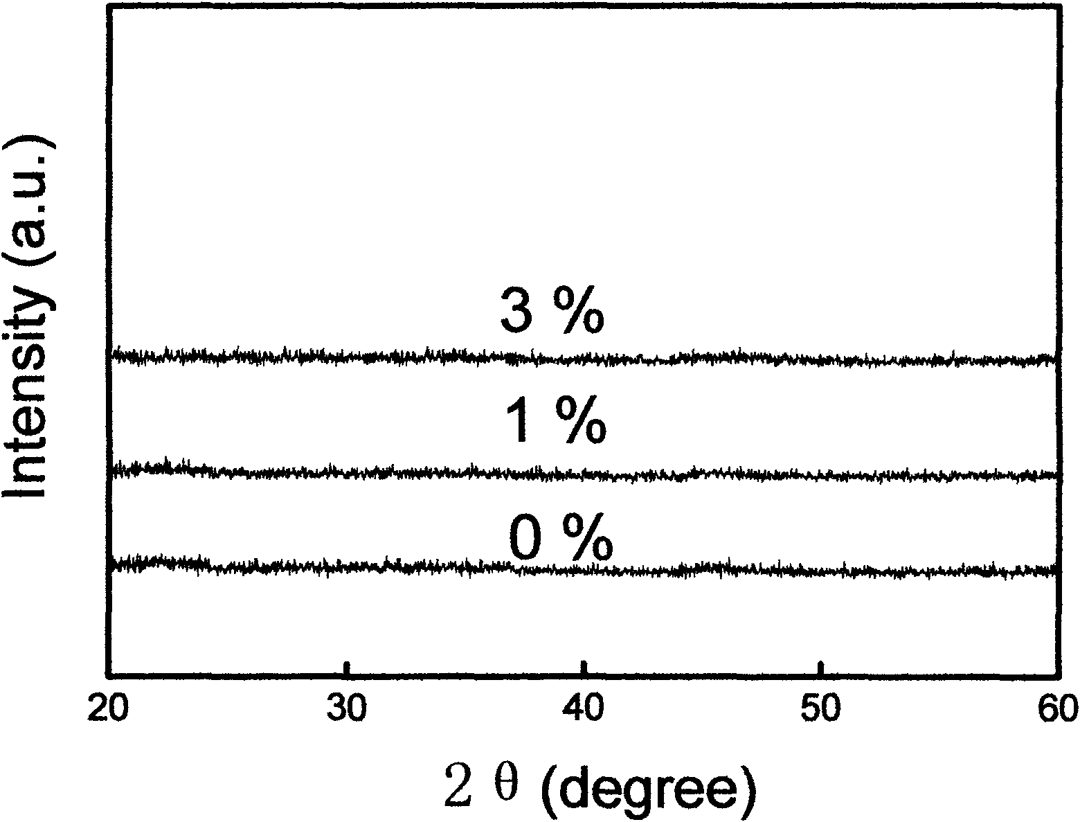
[0039] Select a P-type Si (100) substrate, the resistivity of the silicon wafer is 2-10 Ω cm, the substrate temperature is room temperature, and the Er 2 o 3 and Al 2 o 3 On the P-type Si(100) substrate, the ErAlO amorphous composite oxide film is formed by radio frequency magnetron sputtering. The purity of the mixed ceramic target material is 99.99%, Al 2 o 3 Accounting for 30% molar ratio, RF power is 40W, sputtering gas is Ar and O 2 , oxygen partial pressure ratio P=P(O 2 ) / ((P(O 2 )+P(Ar)) are 0%, 1% and 3%, the working pressure is 1.0Pa, and the P-type (100) silicon wafer with a resistivity of 2-10Ω·cm is ultrasonically cleaned with deionized water for 10 minutes before growth, and then Etch with 1% HF acid for 30 s to remove the natural oxide layer on the surface of the Si substrate, and finally send it into the growth chamber for 30 min...


PUM

PropertyMeasurementUnit
electrical resistivityaaaaaaaaaa
thicknessaaaaaaaaaa
electrical resistanceaaaaaaaaaa

Abstract

The invention discloses a high-k gate dielectric material and a preparation method thereof, belonging to the technical field of semiconductors, in particular to the application field of metallic oxide semiconductor field effect transistors (MOSFET). The high-k gate dielectric material is a composite material of Er2O3-Al2O3 (ErAlO); an ErAlO amorphous grate dielectric composite oxide film is prepared on a P-type Si (100) substrate by an RF magnetron sputtering preparation method by a sputtering target which is a mixed ceramic target of Er2O3 and Al2O3; according to tests, the ErAlO film has favorable thermostability and planeness as well as low leakage current density and can replace SiO2 to become a novel high-k gate dielectric material.

Description

technical field [0001] The invention belongs to the field of semiconductors, in particular to the application field of metal oxide semiconductor field-effect transistors (MOSFETs), in particular to a high-k gate dielectric material and a preparation method thereof. The invention uses radio frequency magnetron sputtering to prepare amorphous Er2O3 - Al2O3 (ErAlO) high-K gate dielectric composite oxide film. The present invention provides a substitute for SiO 2 A new high-k gate dielectric candidate material, and its preparation method is provided. Background technique [0002] With the reduction of transistor feature size in integrated circuits, the current field effect transistor gate dielectric SiO 2 The thickness has been reduced to the nanometer level. At this time, affected by the tunneling effect, the gate leakage current will increase exponentially with the decrease of the thickness of the oxide layer, which becomes a problem that cannot be ignored. One of the solu...

Claims


Application Information

Patent Timeline
Patent Type & Authority Applications(China)
IPC IPC(8): H01L29/51H01L21/28H01L21/283H01L21/336
Inventor 方泽波陈伟
Owner SHAOXING UNIVERSITY
Why Eureka
Try Eureka