GaN-based Single chip white light emitting diode epitaxial material

A technology of light-emitting diodes and epitaxial materials, which is applied in the direction of electrical components, circuits, semiconductor devices, etc., can solve the problems of not being practical, and the white light luminous efficiency of GaN-based white light-emitting diodes is not high enough, so as to reduce dislocations and improve light utilization Efficiency, simplification of the production process and the effect of the process

Inactive Publication Date: 2010-03-31
INST OF PHYSICS - CHINESE ACAD OF SCI
View PDF1 Cites 89 Cited by
  • Summary
  • Abstract
  • Description
  • Claims
  • Application Information

AI Technical Summary

Problems solved by technology

However, the GaN-based white light-emitting diode without phosphor powder conversion still has the defect tha

Method used


Image

  • GaN-based Single chip white light emitting diode epitaxial material
  • GaN-based Single chip white light emitting diode epitaxial material

Examples


Embodiment 1

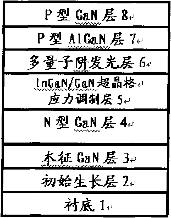
[0030] refer to figure 1 , making a GaN-based single-chip white light-emitting diode epitaxial material of the present invention, its structure is as follows:

[0031] Using sapphire as the substrate 1, a 20nm thick GaN initial growth layer 2, a 200nm intrinsic GaN layer 3, and a 1 μm thick n-type GaN layer 4 (doped Concentration 5×10 18 cm -3 ), 20 cycles of 10nm thick (referring to In 0.1 Ga 0.9 N monolayer thickness) In 0.1 Ga 0.9 N / 10nm thick GaN superlattice stress modulation layer 5, InGaN multi-quantum structure light-emitting layer 6 (composed of barrier layer In 0.05 Ga 0.95 N and quantum well layer In 0.15 Ga 0.85 5 periods of multiple quantum wells composed of N, in which the barrier layer In 0.05 Ga 0.95 The thickness of N is 10nm, the quantum well layer In 0.15 Ga 0.85 N thickness is 3nm), 100nm thick p-type Al 0.2 Ga 0.8 N interlayer 7, 100nm thick p-type GaN layer 8 (doping concentration 3×10 17 cm -3 ), to obtain the GaN-based single-chip white...

Embodiment 2

[0033] refer to figure 1 , make a GaN-based single-chip white light-emitting diode epitaxial material of the present invention: adopt 0.4mm thick SiC as the substrate 1, use metal organic chemical vapor deposition technology (MOCVD) to sequentially grow 100nm thick AlN initial growth on it Layer 2, 0.3 μm thick intrinsic GaN layer 3, 1 μm thick n-type GaN layer 4, 150 nm thick 10 periods of 5 nmIn 0.15 Ga 0.85 N / 10nm thick In 0.05 Ga 0.95 N superlattice stress modulation layer 5, InGaN multi-quantum structure light-emitting layer 6 (composed of barrier layer GaN and quantum well layer In 0.15 Ga 0.85 4 periods of multiple quantum wells composed of N, in which the thickness of the barrier layer GaN is 12nm, and the quantum well layer In 0.15 Ga 0.85 The thickness of N is 3 nm, and the doping concentration of GaN in the barrier layer is 1×10 18 / cm 3 , the doping concentration of the quantum well layer InxGa1-xN layer is 0), 50nm thick p-type Al 0.2 Ga 0.8 N interlayer...

Embodiment 3

[0035] refer to figure 1 , making a GaN-based single-chip white light-emitting diode epitaxial material of the present invention: a 0.3mm thick silicon substrate is used as the substrate 1, and a 200nm thick AlN initial growth layer 2 is sequentially grown on it by molecular beam epitaxy (MBE) , 0.5 μm thick intrinsic GaN layer 3, 0.5 μm thick n-type GaN layer 4, 15 cycles of 1nm In 0.3 Ga 0.7 N / 8nm In 0.05 al 0.02 Ga 0.93 N superlattice stress modulation layer 5, InGaN multi-quantum structure light-emitting layer 6 (composed of barrier layer GaN and quantum well layer In 0.15 Ga 0.85 4 periods of multiple quantum wells composed of N, in which the thickness of the barrier layer GaN is 10nm, and the quantum well layer In 0.15 Ga 0.85 The thickness of N is 3 nm, and the doping concentration of GaN in the barrier layer is 1×10 17 / cm 3 , the quantum well layer In x Ga 1-x The doping concentration of the N layer is 2×10 17 / cm 3 ), 100nm thick p-type Al 0.2 Ga 0.8 N...


PUM

PropertyMeasurementUnit
Thicknessaaaaaaaaaa
Thicknessaaaaaaaaaa
Thicknessaaaaaaaaaa

Abstract

The invention relates to GaN-based Single chip white light emitting diode epitaxial material comprising a substrate and also comprising an initial growth layer, an intrinsic GaN buffer layer, an n-type GaN layer, a stress relaxation layer, an InGaN multiple quantum well structure light emitting layer, a p-type AlGaN sandwich layer and a p-type GaN layer which grow in sequence on the substrate. Thestress relaxation layer is an InGaN/GaN superlattice stress modulation layer which comprises InGaN layers and GaN layers, which are grown alternatively; the InGaN layers and GaN layers have the growth cycle of 6-500 and the corresponding thickness of 10 nm to 3 Mum; and the In components in the InGaN layers are in the range of 1-35 percent. Because the stress-relaxed InGaN/GaN superlattice stressmodulation layer is added between the n-type GaN layer and a multiple quantum light emitting layer, the In segregation effect is strengthened, InGaN quantum dots with different components are formed,and the mixing of different-wave light emitted by the InGaN quantum dots realizes the white light emitting. The cost of the white light emitting diode is reduced radically, the light emitting efficiency and the light using efficiency are increased and the integral performance of the white light emitting diode is improved.

Description

technical field [0001] The invention relates to a white light emitting diode epitaxial material, in particular to an epitaxial material for a white light GaN-based single-chip light emitting diode chip that does not require phosphor powder conversion. Background technique [0002] As a white light source, white light-emitting diodes have many advantages such as high luminous efficiency, short response time, and long life. These advantages determine that it will replace the existing white light source. At present, there are three kinds of manufacturing methods for white light-emitting diodes that are generally accepted: (1) three red, green and blue light-emitting diodes that are separately produced or integrated in a single chip emit light at the same time, thereby mixing white light, (2) The red, green and blue three-color mixed phosphor powder wrapped in the outer layer is excited by the ultraviolet or purple light-emitting diode as the light source, and the three-color ph...

Claims


Application Information

Patent Timeline
IPC IPC(8): H01L33/00
Inventor 陈弘郭丽伟贾海强李卫王文新
Owner INST OF PHYSICS - CHINESE ACAD OF SCI
Why Eureka
Try Eureka