Ultraviolet light-emitting diode based on n-ZnO/n-GaN alloplasm nN node and preparation method thereof

A light-emitting diode and heterogeneous technology, applied in the field of nanomaterials and optoelectronic devices, can solve the problems of high threshold voltage and low luminous intensity, and achieve the effects of reducing threshold voltage, improving performance, and improving ultraviolet luminescence performance

Inactive Publication Date: 2013-04-03
WUHAN UNIV
View PDF2 Cites 0 Cited by
  • Summary
  • Abstract
  • Description
  • Claims
  • Application Information

AI Technical Summary

Problems solved by technology

[0005] The purpose of the present invention is to improve the defects of low luminous intensity and high threshold voltage of traditional ultraviolet light-emitting diodes.

Method used


Image

  • Ultraviolet light-emitting diode based on n-ZnO/n-GaN alloplasm nN node and preparation method thereof
  • Ultraviolet light-emitting diode based on n-ZnO/n-GaN alloplasm nN node and preparation method thereof
  • Ultraviolet light-emitting diode based on n-ZnO/n-GaN alloplasm nN node and preparation method thereof

Examples


preparation example Construction

[0030] (2) Preparation of i-type intermediate layer. RF magnetron sputtering process conditions: The target material is a Mg metal target or a ZnO small ceramic sheet or a ZnO ceramic target stacked on a Mg metal target. The background vacuum during sputtering is better than 10 -3 Pa, the substrate temperature is 150-400°C, the gas pressure during deposition is 0.5-5.0Pa, and the relative oxygen partial pressure is O 2 / (O 2 +Ar)=1 / 5~1 / 2, the sputtering power range is 80~130W, and the sputtering time is 8~15 minutes;

[0031] (3) growing n-type ZnO thin film layer. The condition parameters used in radio frequency magnetron sputtering are: the target material is a ZnO ceramic target. The background vacuum degree during sputtering is better than 5×10 -3 Pa, the substrate temperature is 150-450°C, the gas pressure during deposition is 0.5-5.0Pa, and the relative oxygen partial pressure is O 2 / (O 2 +Ar)=1 / 9~1 / 6, the sputtering power range is 80~130W, and the sputtering tim...

Embodiment 1

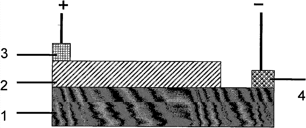
[0037] 1. Substrate cleaning: use n-type gallium nitride / sapphire as the substrate, cut it into a size of 25mm×30mm,

[0038]Use acetone, alcohol, and deionized water to ultrasonically clean for 3 minutes, and finally blow dry with a nitrogen gun.

[0039] 2. Growth of n-type layer ZnO: use radio frequency magnetron sputtering method to deposit ZnO thin film (2) on GaN layer (1). The target material is ZnO ceramic target, and the background vacuum is 1.0×10 -3 Pa, the deposition substrate temperature is 300°C, the gas pressure during deposition is 1.0Pa, and the relative oxygen partial pressure is O 2 / (O 2 +Ar)=1 / 6, power 80W, sputtering time 45 minutes.

[0040] 3. Electrode preparation: Au electrodes (3) were prepared on the surface of the ZnO thin film by DC sputtering method, the substrate temperature was 120° C., and the deposition time was 1 minute. The Al electrode (4) is prepared on the surface of the GaN thin film by thermal evaporation process, and the depositio...

Embodiment 2

[0043] 1. Substrate cleaning: use n-type gallium nitride / sapphire as the substrate, cut it into a size of 25mm×30mm,

[0044] Use acetone, alcohol, and deionized water to ultrasonically clean for 3 minutes, and finally blow dry with a nitrogen gun.

[0045] 2. Growth of n-type layer ZnO: use radio frequency magnetron sputtering method to deposit ZnO thin film (2) on GaN layer (1). The target material is ZnO ceramic target, and the background vacuum is 1.0×10 -3 Pa, the deposition substrate temperature is 150°C, the gas pressure during deposition is 0.5Pa, and the relative oxygen partial pressure is O 2 / (O 2 +Ar)=1 / 9, power 130W, sputtering time 30 minutes.

[0046] 3. Electrode preparation: The Ag electrode (3) was prepared on the surface of the ZnO thin film by DC sputtering method, the substrate temperature was 100° C., and the deposition time was 2 minutes. An In electrode (4) is prepared on the surface of the GaN thin film by a thermal evaporation process, and the dep...


PUM


Abstract

The invention discloses an ultraviolet light-emitting diode based on an n-ZnO / n-GaN alloplasm nN node and a preparation method thereof. The ultraviolet light-emitting diode based on the alloplasm nN node at least comprises an nN node and an ohmic contact electrode, wherein an n-type ZnO film grows on a sapphire substrate on which n-type GaN grows to form the alloplasm nN node, or a middle-layer film firstly grows on a sapphire substrate on which n-type GaN grows, and then the n-type ZnO film grows to form the alloplasm nN node. The diode based on n-ZnO / n-GaN alloplasm nN node, prepared by theinvention has favourable luminous performance and lower threshold voltage with a minimum of 2.5 V, the luminescence wavelength can be about 370 nm, the line width is smaller than 8.8 nm, and the luminous intensity is extremely high.

Description

technical field [0001] The invention belongs to the field of nanometer materials and optoelectronic devices, and in particular relates to an ultraviolet light-emitting diode based on n-ZnO / n-GaN heterogeneous nN junction and a preparation method thereof. Background technique [0002] Zinc oxide (ZnO) is a new type II-VI direct bandgap wide bandgap semiconductor material. The band gap of ZnO is 3.37eV at room temperature, and the emission wavelength is equivalent to the wavelength of near-ultraviolet light, which is very suitable for making short-wavelength light-emitting and photosensitive devices. The lattice structure, unit cell parameters and forbidden band width of ZnO are similar to GaN, and it has a higher melting point and greater exciton binding energy than GaN, and has a lower photoluminescence and stimulated emission threshold. And good electromechanical coupling characteristics, thermal stability and chemical stability. Therefore, it has great potential in the a...

Claims


Application Information

Patent Timeline
Patent Type & Authority Patents(China)
IPC IPC(8): H01L33/26
Inventor 方国家李颂战龙浩莫小明黄晖辉
Owner WUHAN UNIV
Why Eureka
Try Eureka