Method for manufacturing optical waveguide by using azobenzene polymer

An azo polymer, optical waveguide technology, applied in the direction of optical waveguide and light guide, can solve the problems of narrow refractive index change, unable to meet the requirements of the refractive index gradient change of waveguide devices, not too much, etc. The effect of eliminating reactive ion etching and avoiding the use of photoresist

Inactive Publication Date: 2011-04-27
TSINGHUA UNIV
View PDF3 Cites 0 Cited by
  • Summary
  • Abstract
  • Description
  • Claims
  • Application Information

AI Technical Summary

Problems solved by technology

[0004] However, among the polymer film materials that have been reported so far, there are not too many types of materials that can be used for photobleaching to change the refractive index, and most of them require strong ultraviolet exposure to achieve bleaching. For example, Koo, J. et al. .Mater.2002, 14, 5030-5036 and Opt.Mater.2003, 23, 583-592 reported research results, and there are fewer materials that can be bleached under visible light irradiation
On the other hand, most of the existing polymer thin film materials have a relatively narrow range of refractive index change with irradiation conditions, and many of them cannot meet the requirements of waveguide devices for refractive index gradient changes.

Method used


Image

  • Method for manufacturing optical waveguide by using azobenzene polymer
  • Method for manufacturing optical waveguide by using azobenzene polymer
  • Method for manufacturing optical waveguide by using azobenzene polymer

Examples


preparation example Construction

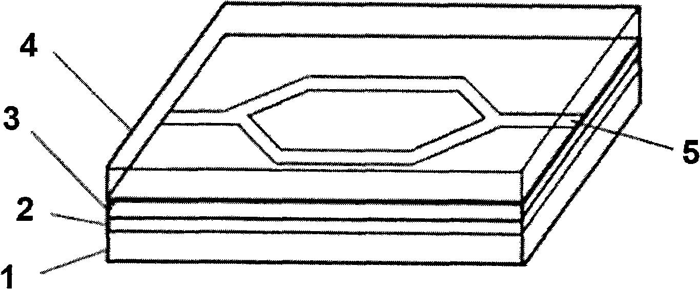
[0030] The method that the present invention proposes to make optical waveguide with azo polymer, the structural representation of the prepared optical waveguide is as follows figure 1 Shown, specific preparation method comprises the following steps:

[0031] (1) cleaning the substrate 1;

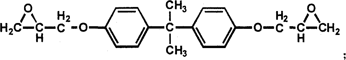
[0032] (2) Mix the epoxy resin prepolymer, isocyanate and N,N-dimethylformamide to obtain a first mixed solution. The mixing mass ratio is: epoxy resin prepolymer:isocyanate:N,N-dimethylformamide=1:0.3-0.9:3-9. The first mixed solution is spin-coated on the above-mentioned cleaned substrate, and dried at a temperature of 60-180° C. for 6-12 hours to obtain a lower cladding layer 2 with a thickness of 1.0-5.0 microns, wherein the epoxy resin The molecular structural formula of the prepolymer is:

[0033]

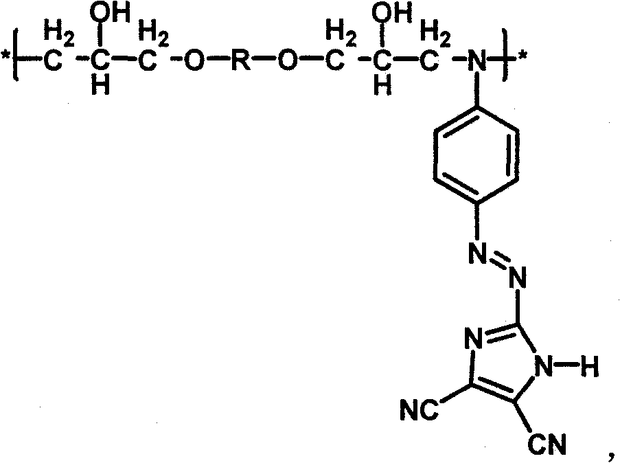
[0034] (3) Mixing the azo polymer, isocyanate and N,N-dimethylformamide to obtain a second mixed solution. The mixing mass ratio is: azo polymer: isocyanate: N, N-dimethylformamide ...

Embodiment 1

[0050] (1) Select silicon as the substrate material, use acetone, ethanol, and water for 15 minutes to sonicate, repeat twice, and finally blow dry with N2 gas for later use;

[0051] (2) Mix the epoxy resin prepolymer, isocyanate and N,N-dimethylformamide to obtain a first mixed solution. The mixing mass ratio is: epoxy resin prepolymer:isocyanate:N,N-dimethylformamide=1:0.6:6.4. The first mixed solution was spin-coated on the above-mentioned cleaned substrate, and dried at 60° C. for 12 hours to obtain a lower cladding layer with a thickness of 3.0 μm, wherein the molecular structural formula of the epoxy resin prepolymer is :

[0052]

[0053] (3) Azopolymer, isocyanate and N, N-dimethylformamide are mixed to obtain the second mixed solution, and the mass ratio of mixing is: azopolymer: isocyanate: N, N-dimethylformamide Amide=1:0.25:12, the second mixed solution is spin-coated on the above-mentioned lower cladding layer, and dried at 60°C for 12 hours to obtain a core...

Embodiment 2

[0060] (1) Select quartz glass as the substrate material, use acetone, ethanol, and water to sonicate for 15 minutes, repeat twice, and finally dry it with N2 gas for later use;

[0061] (2) Mix the epoxy resin prepolymer, isocyanate and N,N-dimethylformamide to obtain a first mixed solution. The mixing mass ratio is: epoxy resin prepolymer:isocyanate:N,N-dimethylformamide=1:0.6:6.4. The first mixed solution was spin-coated on the above-mentioned cleaned substrate, and dried at 60° C. for 12 hours to obtain a lower cladding layer with a thickness of 3.0 μm, wherein the molecular structural formula of the epoxy resin prepolymer is :

[0062]

[0063] (3) Azopolymer, isocyanate and N, N-dimethylformamide are mixed to obtain the second mixed solution, and the mass ratio of mixing is: azopolymer: isocyanate: N, N-dimethylformamide Amide=1:0.25:12, the second mixed solution is spin-coated on the above-mentioned lower cladding layer, and dried at 60°C for 12 hours to obtain a c...


PUM


Abstract

The invention relates to a method for manufacturing optical waveguide by using an azobenzene polymer, and belongs to the technical field of optical device manufacturing. The method comprises the following steps: firstly, cleaning an underlayer; mixing an epoxy resin prepolymer, isocyanate and N,N-Dimethylformamide so as to obtain first blended solution, then spin-coating the first blended solution on the cleaned underlayer to obtain a lower cladding; mixing the azobenzene polymer, isocyanate and N,N-Dimethylformamide so as to obtain second blended solution, then spin-coating the second blended solution on the lower cladding to obtain a sandwich layer; placing a mask on the sandwich layer, irradiating the mask with a laser so as to form the optical waveguide; and coating a curing glue on an upper cladding of the optical waveguide. The method has the advantages of simple manufacturing process, easily controlled quality and low product cost.

Description

technical field [0001] The invention relates to a method for making an optical waveguide by using an azo polymer, and belongs to the technical field of optical device preparation. Background technique [0002] Optical waveguide fabrication technology is the core technology of planar integrated optical devices. The manufacture of high-performance power splitters, optical amplifiers, directional couplers, and electro-optical modulators in integrated optical circuits all depend on the development and optimization of optical waveguide technology. Materials that can currently be used to make optical waveguides include: lithium niobate (LiNbO3), III-V semiconductor compounds, silicon dioxide (SiO2), SOI (Silicon-on-Insulator, silicon on insulator), polymer (Polymer) and glass . The conventional manufacturing processes mainly include etching and diffusion. Among the optical waveguides using the etching process, the buried silicon-based silica optical waveguide is widely used at ...

Claims


Application Information

Patent Timeline
Patent Type & Authority Patents(China)
IPC IPC(8): G02B6/13
Inventor 叶钢和亚宁曲欣王晓林白一鸣吴伯瑜王晓工
Owner TSINGHUA UNIV
Why Eureka
Try Eureka