Method for preparing cubic indium oxide single-crystal film on yttrium-doped zirconia substrate

A technology of single crystal thin film and cubic structure, applied in gaseous chemical plating, metal material coating process, coating, etc., can solve the problems of material stability, low carrier mobility, unsuitable for industrial production, etc., to achieve Good uniformity and repeatability, broad application prospects, and excellent photoelectric performance

Inactive Publication Date: 2010-08-04
SHANDONG UNIV
View PDF4 Cites 4 Cited by
  • Summary
  • Abstract
  • Description
  • Claims
  • Application Information

AI Technical Summary

Problems solved by technology

Intrinsic indium oxide is an n-type semiconductor material, while indium oxide films prepared by conventional methods generally have a polycrystalline structure, and there are a large number of defects and grain boundaries inside the film, which have a strong scattering effect on carriers, making current carriers Submobility is low
[0005] (2) Due to the existence of a large number of oxygen vacancy defects in polycrystalline indium oxide and the oxygen adsorption at the grain boundary, the stability of the material is greatly affected
[0006] (3) Although molecular beam epitaxy (MBE) and pulsed laser deposition (PLD) methods can be used to prepare indium oxide single crystal epitaxial thin films on substrate materials that match the indium oxide lattice, the growth rate is slow and the film formation is slow. Small area, not suitable for industrial production
However, the disadvantage of this invention is that the α-Al with hexagonal structure 2 o 3 There are three equivalent directions on the C-plane of the substrate, so twins and domain structures inevitably appear in the epitaxially grown single crystal film, which reduces the carrier mobility of the film

Method used


Image

  • Method for preparing cubic indium oxide single-crystal film on yttrium-doped zirconia substrate
  • Method for preparing cubic indium oxide single-crystal film on yttrium-doped zirconia substrate
  • Method for preparing cubic indium oxide single-crystal film on yttrium-doped zirconia substrate

Examples


Embodiment 1

[0057] Example 1: Preparation of Cubic Indium Oxide Single Crystal Thin Film Material by MOCVD Technology

[0058] (1) First pump the reaction chamber of the MOCVD equipment to a high vacuum state of 5×10 -4 Pa, heat the substrate to 650°C;

[0059] (2) Open the valve of the nitrogen cylinder and feed nitrogen into the reaction chamber (background N 2 450sccm) for 20 minutes, the reaction chamber pressure was stabilized at 40Torr;

[0060] (3) Open the valve of the oxygen cylinder, adjust the flow rate of oxygen to 50 sccm, and keep it for 5 minutes;

[0061] (4) Set the pressure of the organometallic source bottle to 240 Torr, open the valve of the indium source bottle, adjust the flow rate of the carrier gas (nitrogen) to 25 sccm, and keep for 5 minutes;

[0062] (5) Pass oxygen and organometallic indium sources into the reaction chamber at the same time, and keep the film growth time at 180 minutes;

[0063] (6) After the reaction, close the valves of the indium source ...

Embodiment 2

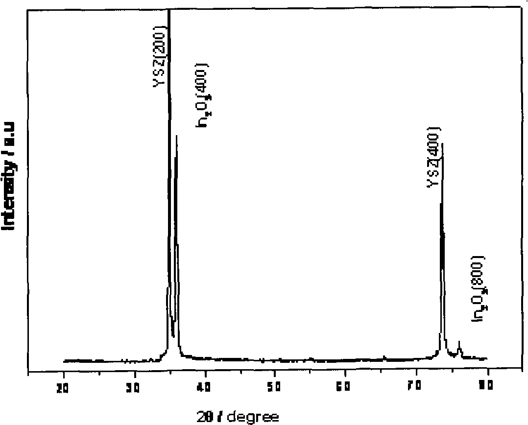
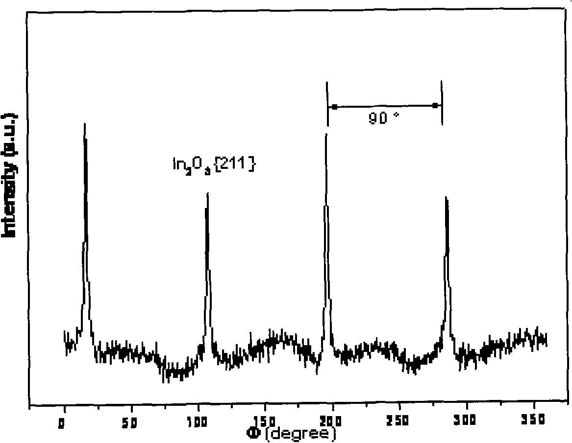
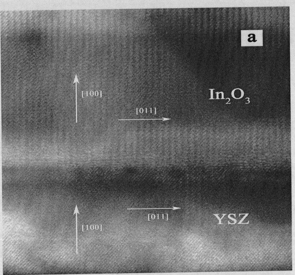
[0068] Monocrystalline indium oxide thin film material was prepared by MOCVD technology, and the preparation process was the same as in Example 1, except that the reaction chamber pressure was 30 Torr, the substrate temperature (growth temperature) was 700° C., and the film growth time was 180 minutes. Using polished YSZ (100) as the substrate material, the prepared indium oxide film has a single crystal structure, the thickness of the film is 157nm, and the carrier mobility of the film is 61.2cm 2 V -1 the s -1 .


PUM

PropertyMeasurementUnit
thicknessaaaaaaaaaa
thicknessaaaaaaaaaa
thicknessaaaaaaaaaa

Abstract

The invention relates to a preparation method for a cubic indium oxide single-crystal epitaxial film. By adopting the organic metal chemical gas deposition technology, trimethylindium is used as an organic metal source, nitrogen is used as carrier gas, oxygen is used as oxidizing gas and an organic metal chemical gas deposition device is used to epitaxially grow indium oxide single-crystal film on an yttrium-doped zirconia substrate under vacuum conditions. The film is the epitaxial material with single-crystal structure, twin crystals and domain structures do not exist in the film, and the mobility of the current carrier of the film is higher than 61.2 cm<2>V<-1>s<-1>.

Description

technical field [0001] The invention relates to a method for preparing a cubic indium oxide single crystal thin film, belonging to the technical field of semiconductor optoelectronic materials. Background technique [0002] Indium oxide with a cubic structure (In 2 o 3 ) is a wide bandgap semiconductor material with a bandgap width of about 3.7eV at room temperature, and has the advantages of low preparation temperature and stable physical and chemical properties. At present, indium oxide thin film materials are mainly used for transparent electrodes of thin-film solar cells and flat-panel displays. High-quality indium oxide single crystal thin films are important materials for preparing transparent and ultraviolet optoelectronic devices. [0003] At present, the following problems exist in the preparation of indium oxide thin films by conventional methods: [0004] (1) Indium oxide transparent conductive films prepared by traditional methods such as magnetron sputtering ...

Claims


Application Information

Patent Timeline
Patent Type & Authority Applications(China)
IPC IPC(8): C23C16/40C23C16/455
Inventor 马瑾孔令沂栾彩娜
Owner SHANDONG UNIV
Why Eureka
Try Eureka